Integrated circuit packages including damming and change protection cover for harsh environments

a technology of integrated circuits and protective covers, which is applied in the direction of printed circuit components, printed circuit casings/cabinets/drawers, printed circuit manufacturing, etc., can solve the problems of lateral shock and vibration, and the temporary lifting off of drill bits from the formation, so as to prevent the migration of conformal coatings and/or encapsulation materials. , to eliminate static charge problems, improve the reworkability of downhole electronic assemblies

Inactive Publication Date: 2009-11-10
SCHLUMBERGER TECH CORP
View PDF11 Cites 3 Cited by
  • Summary
  • Abstract
  • Description
  • Claims
  • Application Information

AI Technical Summary

Benefits of technology

[0012]Exemplary embodiments of the present invention advantageously provide several technical advantages. For example, as stated above, exemplary embodiments of this invention seal the integrated circuit leads in a cavity between the circuit board, the integrated circuit body, and an inner surface of the damming boot, thereby substantially preventing conformal coating and / or encapsulation materials from migrating under the integrated circuit. The use of damming boots in accordance with this invention obviates the need for the above mentioned caulking and / or taping procedures. As such, the invention advantageously tends to eliminate static charge problems associated with the use of conventional caulks and tapes.
[0013]The present invention also tends to advantageously improve the reworkability of downhole electronic assemblies. The damming boot(s) may typically be quickly and easily removed from the integrated circuit and the circuit board (even after encapsulation thereof). Moreover, protection of the integrated circuit leads in the aforementioned cavity eliminates the need to remove caulking, tape, conformal coating, and / or encapsulation material from the leads. As a result, downhole electronic assemblies, including sensitive leads and solder joints, may be visually inspected and / or reworked quickly and efficiently, producing less scrap and commonly enabling circuit board and integrated circuit components to be repaired and re-used multiple times.
[0014]The present invention has also been found to advantageously improve the shock and vibration resistance of various electronic assemblies used in downhole tools. In particular, incidents of failure to the integrated circuit leads and solder joints may be reduced, thereby improving downhole tool reliability and reducing costly trips into and out of the borehole.

Problems solved by technology

It is well known in the art that severe dynamic conditions are often encountered during drilling.
Bit bounce includes axial vibration of the drill string, often resulting in temporary lift off of the drill bit from the formation (“bouncing” of the drill bit off the bottom of the borehole).
Bit bounce, lateral shock and vibration, and stick / slip are commonly recognized as leading causes of electronic failures in downhole tools.
These electronic failures often result in costly trips (tripping the drill string in and out of the borehole) to repair or replace damaged tools and / or tool components.
One drawback with encapsulation processes is that it is difficult to access and repair an electronic assembly once it has been encapsulated.
While the encapsulating material can be removed, or partially removed, from the electronic assembly, its removal is time consuming and difficult.
Removal of the encapsulating layer or layers also often causes further damage to the electronic assembly (e.g., broken leads and / or solder joints).
Another drawback of encapsulation processes is that during encapsulation conformal coating and / or elastomeric encapsulation materials commonly migrate underneath electronic components mounted on the circuit board.
Expansion and contraction of these materials with changing temperatures (e.g., during use of a downhole tool in a borehole) is known to fatigue, or even fracture, solder joints, thereby causing failure of the electronic assembly.
While various methods have been employed to overcome the above described problems associated with encapsulation, these methods are not without their own drawbacks.
While these approaches can be somewhat effective at preventing ingress of the encapsulating materials, they tend to be time consuming and therefore expensive.
Both approaches are also known to be susceptible to the build up of static charges that can cause reliability problems and even failure of sensitive integrated circuits.
For example, installation and removal of tape from the component leads is known to sometimes cause large and damaging static charges.
The caulking material also tends to further exacerbate difficulties in accessing and repairing an encapsulated assembly.
While this approach might be expected to overcome the above described difficulties associated with encapsulation, it is not without its own difficulties.
One particular difficulty is that printed electronic assemblies (including the printed circuit boards and electronic components / integrated circuits soldered thereto) do not typically have tight size or placement tolerances.
This difficulty may be exacerbated by intermediate fabrication steps such as the aforementioned taping and / or caulking of the component leads.
As such, there is difficulty in achieving a consistent snug fit of the pre-forms about the electronic assemblies.
This tends to reduce the effectiveness of the vibration and shock isolation afforded by the molded perform since the electronic assembly can vibrate in the molded perform if it is not held snugly therein.
The result can be more frequent failure of electronic components downhole.
Such resizing is time consuming and results in an unacceptably high degree of variability in the “snugness” of the fit.

Method used


Image

  • Integrated circuit packages including damming and change protection cover for harsh environments
  • Integrated circuit packages including damming and change protection cover for harsh environments
  • Integrated circuit packages including damming and change protection cover for harsh environments

Examples


Embodiment Construction

[0027]Referring first to FIGS. 1 through 7, it will be understood that features or aspects of the exemplary embodiments illustrated may be shown from various views. Where such features or aspects are common to particular views, they are labeled using the same reference numeral. Thus, a feature or aspect labeled with a particular reference numeral on one view in FIGS. 1 through 7 may be described herein with respect to that reference numeral shown on other views.

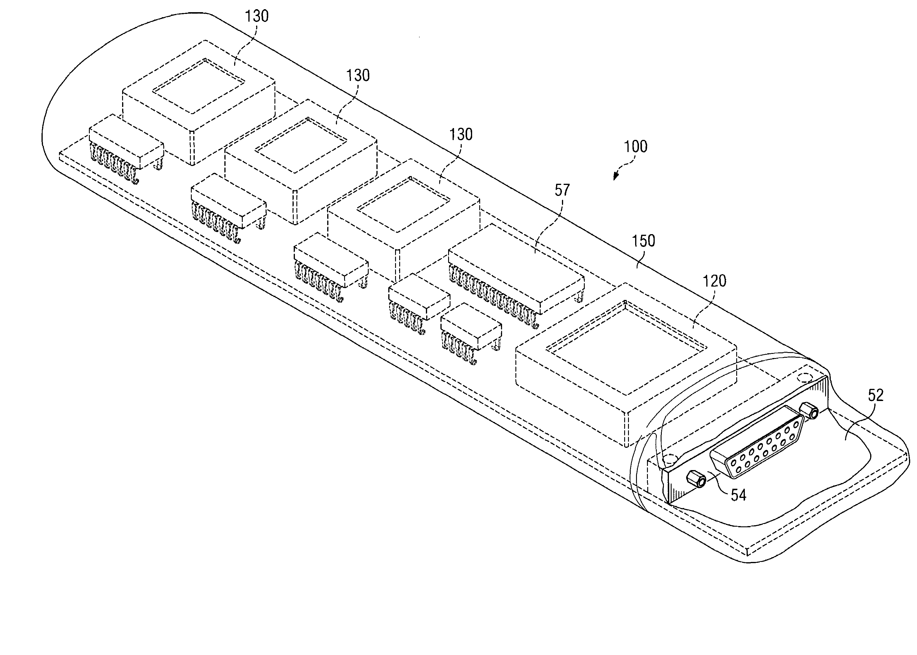
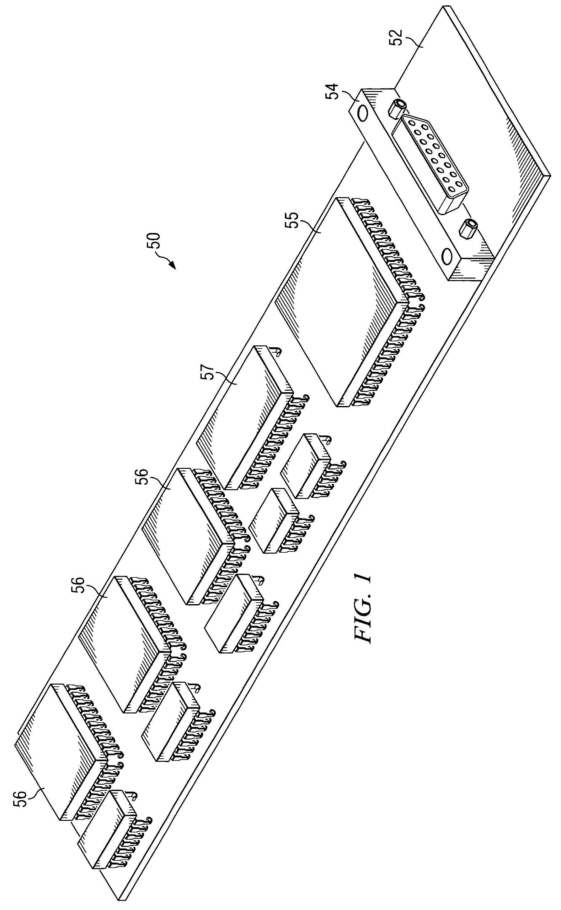
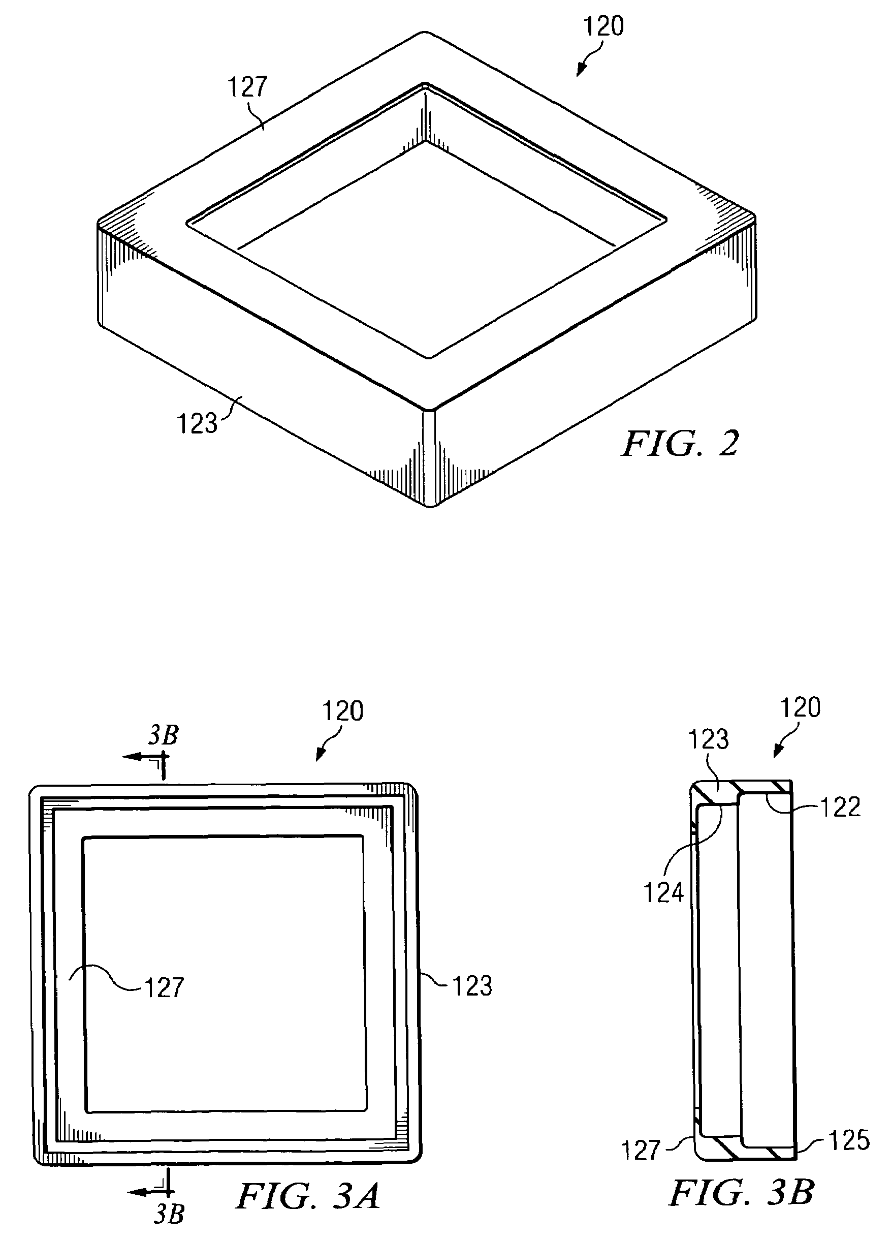
[0028]Turning now to FIG. 1, an exemplary electronic assembly 50 upon which exemplary damming boot embodiments 120 (FIG. 2) of this invention may be deployed. Electronic assembly 50 includes a circuit board 52 (such as a conventional printed circuit board) having a plurality of integrated circuit components 55, 56, and 57 soldered thereto. The assembly 50 further includes an electronic connector 54 for making electronic connection to various other downhole devices. Electronic assembly 50 (and therefore circuit board 52) may b...


PUM


Abstract

An electronic assembly for use in a downhole tool includes a damming boot deployed about at least one integrated circuit component on a circuit board. The boot is disposed to house the integrated circuit leads and solder joints in a substantially sealed cavity between the circuit board, the integrated circuit body, and an inner surface of the damming boot. The boot is also disposed to support the integrated circuit body and thereby improve the shock and vibration resistance of various electronic assemblies used in downhole tools. The invention also tends to improve the reworkability of downhole electronic assemblies.

Description

RELATED APPLICATIONS[0001]None.FIELD OF THE INVENTION[0002]This invention relates generally to integrated circuit board packages for use in downhole tools, and in particular to an integrated circuit board for use in a downhole tool having at least one damming boot deployed about an electronic component (integrated circuit) deployed on the circuit board.BACKGROUND OF THE INVENTION[0003]In recent years there has been a marked increase in the sophistication of downhole tools, and in particular, downhole tools deployed in the bottom hole assembly (BHA) of a drill string. A typical BHA commonly includes, for example, one or more logging while drilling (LWD) and / or measurement while drilling (MWD) tools. Such tools are known to include various electronic sensors such as gamma ray sensors, neutron sensors, resistivity sensors, formation pressure and temperature sensors, ultrasonic sensors, audio-frequency acoustic sensors, magnetic sensors, acceleration sensors, and the like, as well as el...

Claims


Application Information

Patent Timeline
Patent Type & Authority Patents(United States)
IPC IPC(8): H01L23/28
CPCH05K3/301H05K5/0213H05K3/284H05K2203/304H05K2201/10689H05K2201/2018H05K5/0209
Inventor HANLEY, HUGH PATTON
Owner SCHLUMBERGER TECH CORP
Why Eureka
Try Eureka