Semiconductor memory device

a memory device and semiconductor technology, applied in semiconductor devices, electrical devices, instruments, etc., can solve problems such as difficult control of leakage, and achieve the effects of reducing leakage from memory cells, and effectively lengthening the channel

Active Publication Date: 2009-11-17
RENESAS ELECTRONICS CORP
View PDF3 Cites 5 Cited by
  • Summary
  • Abstract
  • Description
  • Claims
  • Application Information

AI Technical Summary

Benefits of technology

[0014]Accordingly, it is an object of the present invention to reduce leak off as the memory cell is made more minute.
[0020]With this invention (first to fourth aspects; claims 1 to 14) it is possible to reduce leak off from the memory cell even when a positive voltage is applied to the selector gate 203. The reason for that is the channel (channel near the sidewall of the floating gate) exists in the height direction even when the cell size is reduced. This makes it possible to effectively lengthen the channel, so it is possible to reduce leak off from the memory cell.
[0021]With this invention (first to fourth aspects; claims 1 to 14) punch through across the drain and source (across the inversion layer and diffusion area) during writing is suppressed. The reason is that the first diffusion area and second diffusion area on the drain side are located such that they are physically lower than the inversion layer on the source side, so it is possible to set the impurity density of the substrate below the floating gate (area between the inversion layer and diffusion area) without affecting the impurity density of the substrate below the selector gate (area where the inversion layer is formed). Also, setting the impurity density of the substrate below the floating gate (area between the inversion layer and diffusion area), so that it is denser than the impurity density of the substrate below the selector gate (area where the inversion layer is formed), is very effective in suppressing punch through. Moreover, the ON current Ion of the memory cell is improved. The reason is that since it is possible to make the impurity density of the substrate below the selector gate (area where the inversion layer is formed) less dense than the impurity density of the substrate below the floating gate (area between the inversion layer and diffusion area), it is possible to lower the channel resistance below the selector gate. In other words, together with being able to prevent punch through by increasing the impurity density of the substrate below the floating gate (area between the inversion layer and diffusion area), it is possible to lower the threshold value of the selector gate by decreasing the impurity density of the substrate below the selector gate (area where the inversion layer is formed), and it is possible to lower the channel resistance of the selector gate. This makes it possible to improve the current when reading a memory cell.

Problems solved by technology

First, as a cell is made more compact, the leak off from the memory cell increases when a positive voltage is applied to the selector gate 203. The reason for this is that the channel length between the inversion layer 220, which is formed below the selector gate 203, and the second diffusion layer 207b become shorter in proportion to the reduction of the cell size, thus making it difficult to control leak off.
Second, when trying to control punch through between the inversion layer 220 and the second diffusion area 207b during the writing operation, the ON current Ion stops flowing. The reason for this is that because the inversion layer 220 and the second diffusion layer 207b are located at the same level on the substrate 201, when the cell is made more minute, it becomes difficult to separate the impurity density in the well 201b of the substrate 201 below the selector gate 203 and the impurity density in the well 201b of the substrate 201 below the floating gate 206 (area between the inversion layer 220 and the second diffusion area 207b) and to form the cell, so there is a trade off between whether to suppress punch through or improve the ON current Ion. In other words, there is a trade off that in order to suppress punch through, it is necessary to increase the impurity density in the well 201b of the substrate 201 below the floating gate 206 (area between the inversion layer 220 and second diffusion area 207b), however, the threshold voltage value of the selector gate transistor increases, and there is a drop in current when reading. Thus there is much to be desired in the art.

Method used


Image

  • Semiconductor memory device
  • Semiconductor memory device
  • Semiconductor memory device

Examples


embodiment 1

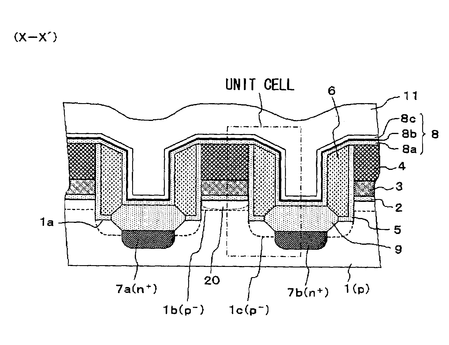
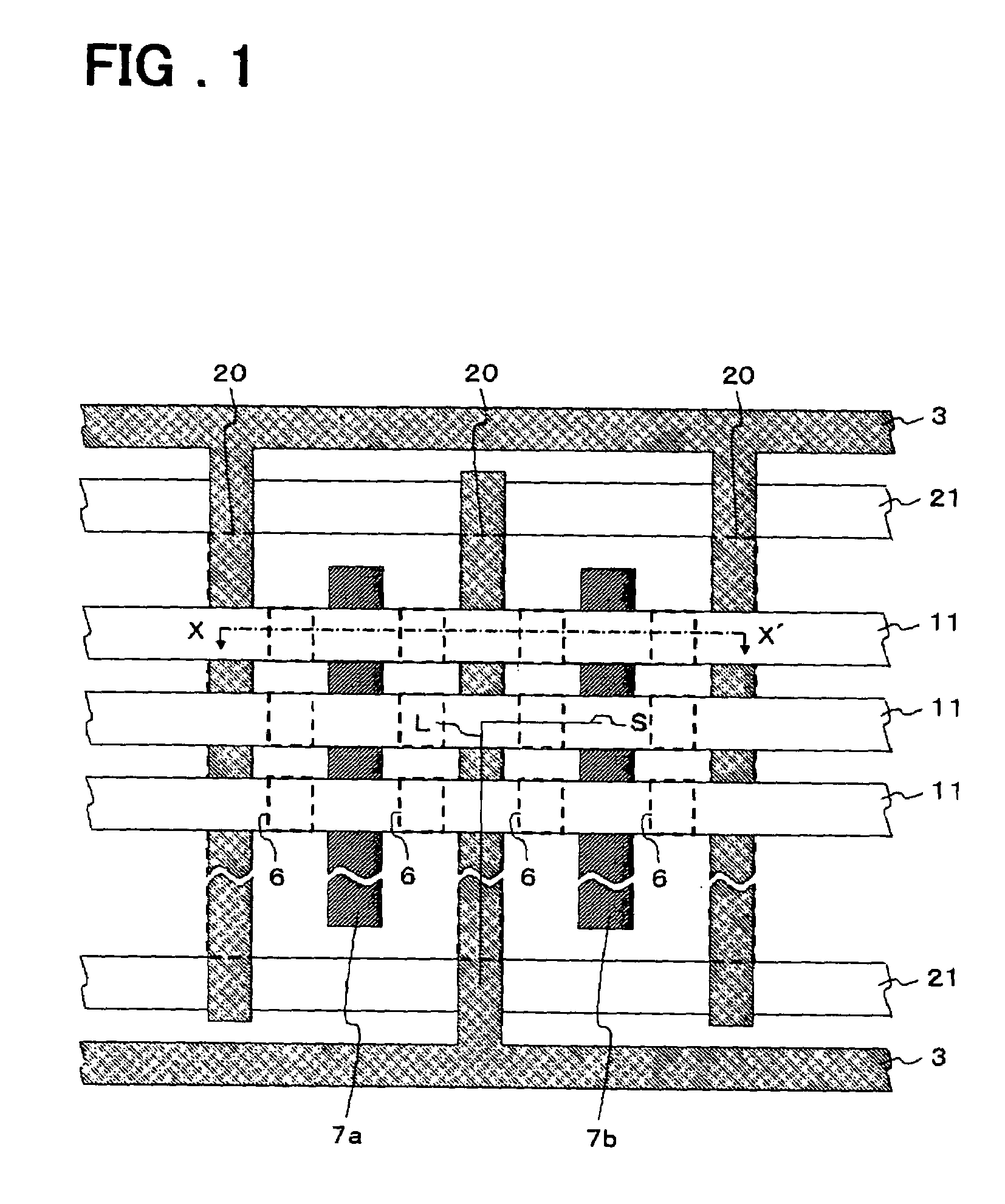
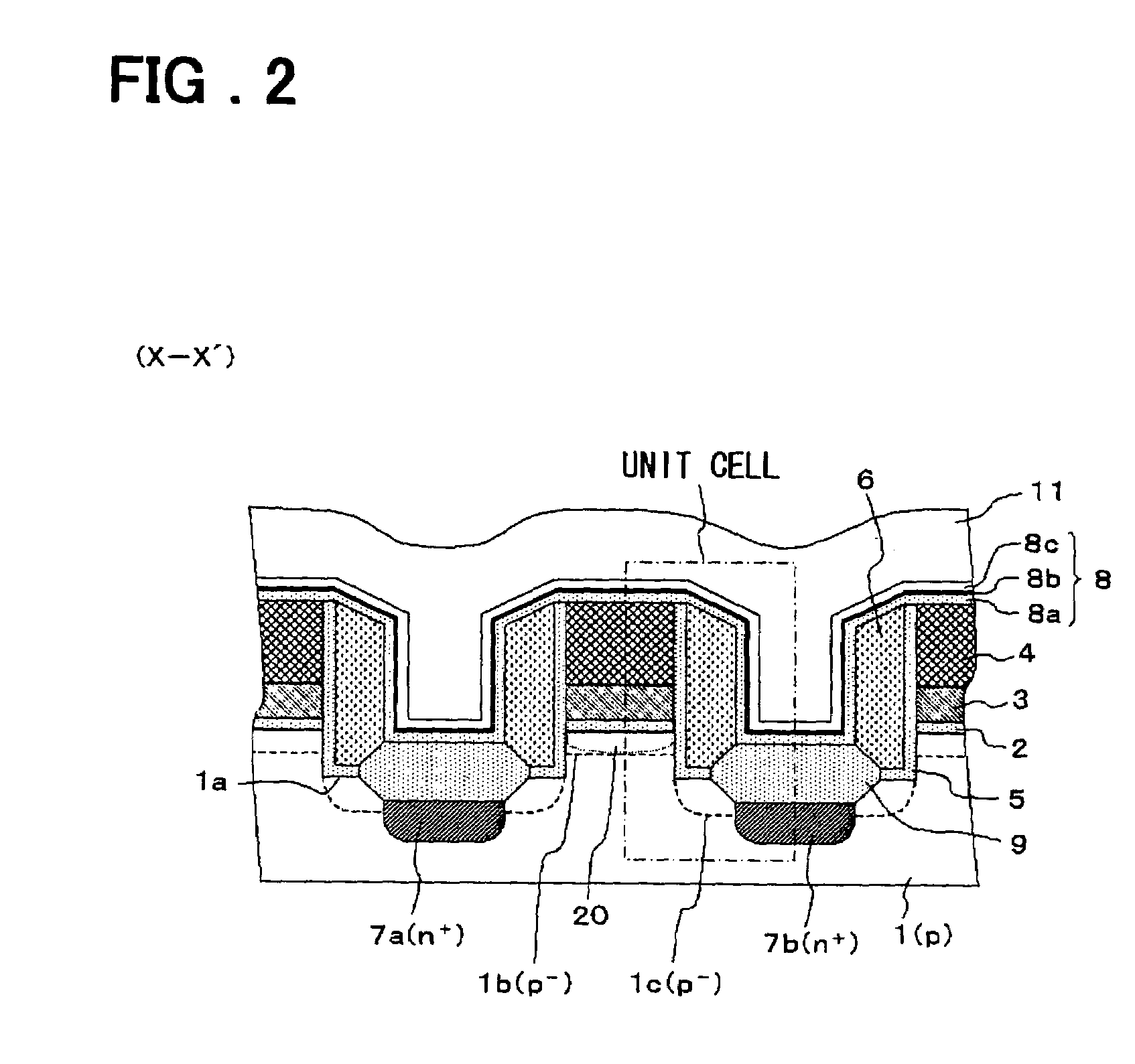
[0041]The semiconductor-memory device of a first embodiment of the invention will be explained using the drawings. FIG. 1 is a partial plan view that schematically shows the construction of the semiconductor-memory device of a first embodiment of the invention; and FIG. 2 is a partial cross-sectional view of the section X-X′ in FIG. 1 that schematically shows the construction of the semiconductor-memory device of a first embodiment of the invention. FIG. 1 shows a semiconductor-memory device that comprises a plurality of memory cells, however, here only one of those memory cells will be explained.

[0042]The semiconductor-memory device is a non-volatile semiconductor-memory device that stores 2 bits of information per cell. The semiconductor-memory device comprises: a substrate 1, insulating film 2, selector gates 3, insulating film 4, insulating film 5, floating gates 6, first diffusion areas 7a, second diffusion areas 7b, insulating film 8, insulating film 9, control gates 11 and th...


PUM


Abstract

A semiconductor-memory device that reduces leak off due to miniaturization of memory cells, and comprises as a single unit cell: a substrate 1 having a trench section 1a; a selector gate 3 that is located via an insulating film 2 on the substrate adjacent to the trench section 1a; a first well 1b that is formed on the surface of the substrate 1 below the selector gate 3; a floating gate 6 that is located via an insulating film 8a on the surface of the bottom section and sidewall section of the trench section 1a; a second well 1c that is formed on the surface of the bottom section of the trench section 1a below the floating gate 6; a first diffusion area 7a that is formed on the surface of the bottom section of the trench section 1a; and a control gate 11 located via an insulating film 8 on top of the floating gate 6; and where the area near the sidewall surface and bottom surface of the trench section 1a forms a channel in the selector gate 3; and the impurity density of the first well 1b is not more than the impurity density of the second well 1c.

Description

FIELD OF THE INVENTION[0001]This invention relates to a semiconductor-memory device having cell transistors, and to the manufacturing method thereof, and particularly to a semiconductor-memory device, which stores a plurality of bits of information per cell, and to the manufacturing method thereof.BACKGROUND OF THE INVENTION[0002]Among conventional semiconductor-memory devices, a non-volatile semiconductor-memory device having cell transistors as shown in FIG. 14 is known as a non-volatile semiconductor-memory device that stores a plurality of bits of information per cell (prior art 1). The non-volatile semiconductor-memory device of prior art 1 comprises: two strip-shaped reverse-conductive areas 123a, 123b that are formed on the top layer of a semiconductor substrate 121, on opposite sides of a strip-shaped conductive semiconductor layer 124a; a first floating gate 127a that is formed via an insulating film 122a such that it extends from the top of one of the reverse-conductive ar...

Claims


Application Information

Patent Timeline
Patent Type & Authority Patents(United States)
IPC IPC(8): H01L29/788
CPCH01L27/115H01L27/11521H01L29/7885H01L27/11526H01L27/11534H01L29/42328H01L27/11524G11C16/0433H10B69/00H10B41/43H10B41/35H10B41/30H10B41/40
Inventor KUBOYAMA, KENICHIKANAMORI, KOHJI
Owner RENESAS ELECTRONICS CORP
Why Eureka
Try Eureka