
Thin-film transistor with semiconductor layer and off-leak current characteristics

a thin film transistor and semiconductor layer technology, applied in the direction of optics, coupling device connections, instruments, etc., can solve the problems of increasing leak current (optical leak current) to a high level, reducing the write voltage that is being maintained, and reducing the contrast of the screen, so as to achieve the effect of improving reliability and reducing fabrication costs

Inactive Publication Date: 2009-12-15
VISTA PEAK VENTURES LLC
View PDF13 Cites 0 Cited by
  • Summary
  • Abstract
  • Description
  • Claims
  • Application Information

AI Technical Summary

Benefits of technology

[0026]It is an object of the present invention to provide a thin-film transistor that can provide lower fabrication costs and increased reliability.
[0028]In the above-described thin-film transistor, prescribing the average thickness of the semiconductor layer of each thin-film transistor to limit the amount of shift in the OFF-leak current characteristic can prevent narrowing of the range of setting of the back-gate voltage.
[0029]Alternatively, when the average film thickness of the semiconductor layer is relatively thick and the range of setting the back-gate voltage narrows due to the existence of a distribution of film thicknesses, narrowing of the range of setting the back-gate voltage can be prevented by prescribing the rate of occurrence of each region having a different film thickness with respect to the channel width direction.
[0030]Accordingly, a thin-film transistor can be obtained in which the effect of back-gate voltage upon the operation of the thin-film transistor can be suppressed to a minimum, whereby a product can be obtained in which display defects are eliminated and reliability is increased. In addition, the elimination of the need for an expensive voltage generation circuit suppresses increase in the cost of the product.

Problems solved by technology

As a result, there is the problem that in an active matrix liquid crystal display device that is used as a liquid crystal light valve, carrier is generated in thin-film transistors due to photoexcitation, thereby increasing leak current (optical leak current) to a high level.
When the optical leak current is great, however, the write voltage that is being maintained will drop, and the screen contrast therefore will also drop.
As a result, the problem occurs that the open area ratio of the pixels cannot be increased.
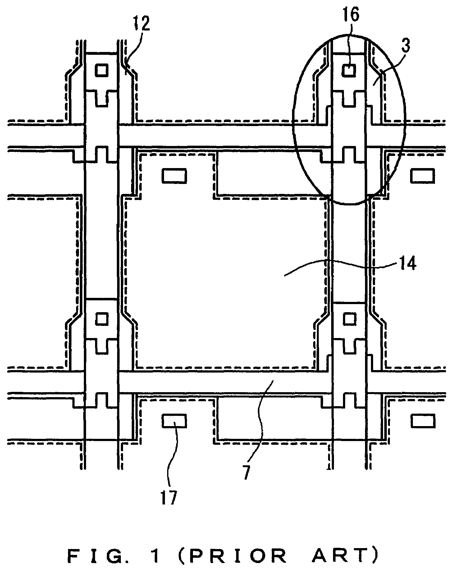
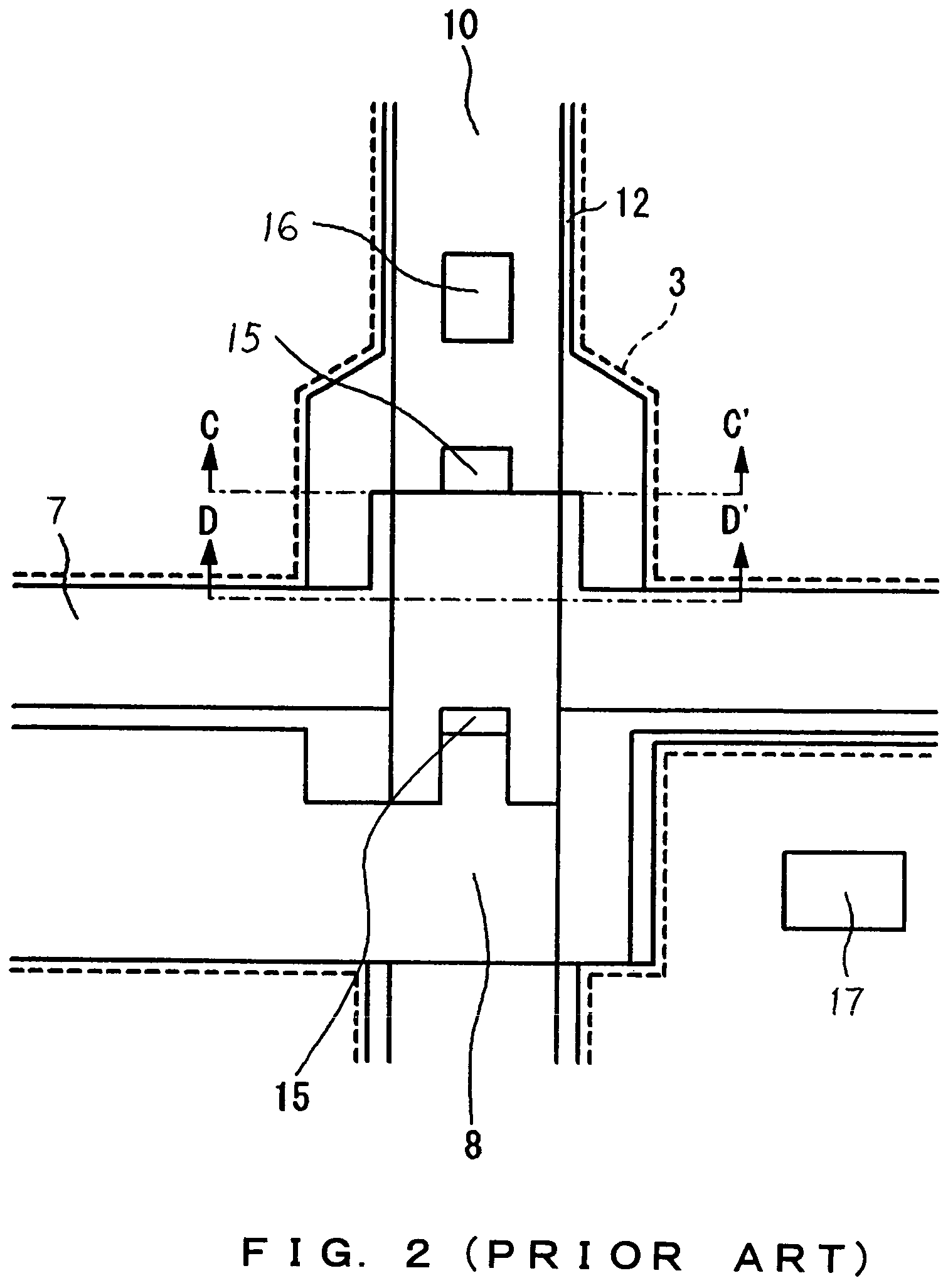
However, an adequate countermeasure has not been found for blocking the diffuse reflection of light that also occurs within the substrates such as shown in FIGS. 3A and 3B.
The leak current in a TFT in which the back-gate voltage diverges from the optimum value increases markedly and therefore produces display defects in the corresponding pixels of the liquid crystal display device and lowers reliability.
In addition, accurately setting the back-gate voltage to a desired voltage necessitates the use of an expensive voltage generation circuit, which raises the additional problem of increased fabrication cost.

Method used


Image

  • Thin-film transistor with semiconductor layer and off-leak current characteristics
  • Thin-film transistor with semiconductor layer and off-leak current characteristics
  • Thin-film transistor with semiconductor layer and off-leak current characteristics

Examples


Embodiment Construction

[0042]Explanation next regards the present invention with reference to the accompanying drawings.

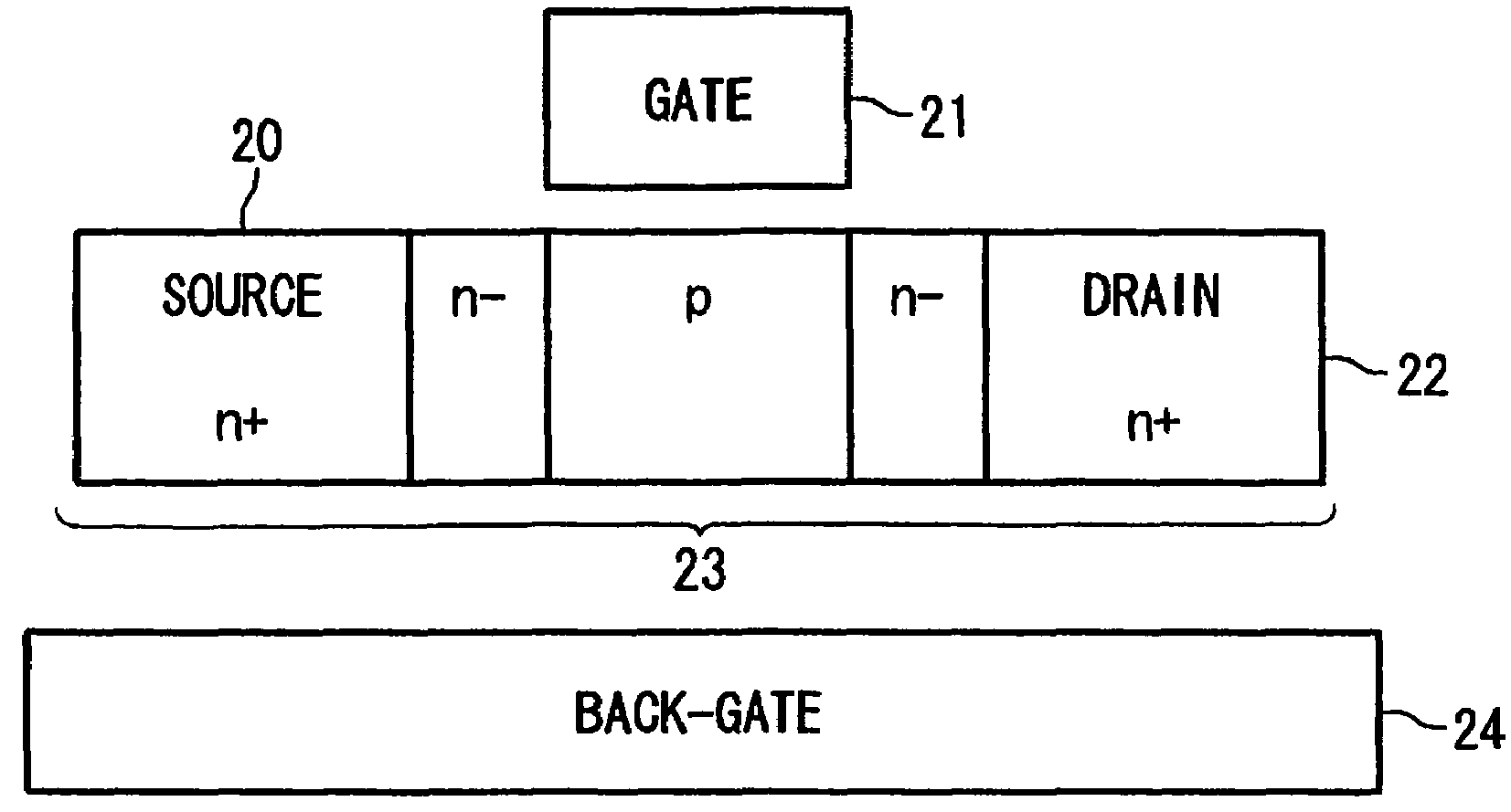
[0043]The following explanation takes as an example of a TFT the configuration shown in FIG. 4 having: silicon layer (semiconductor layer) 23 that is provided with a channel portion (p), LDD regions 23 (n−), source (SOURCE) 20, and drain (DRAIN) 22; gate (GATE) electrode 21 that is formed on silicon layer 23 with a gate insulating film (not shown) interposed; and back-gate (BACK-GATE) 24 that is formed under silicon layer 23 with an interlayer insulating film (not shown) interposed. Back-gate 24 corresponds to lower light-shield film 3 that is arranged in the TFT formation region of the above-described liquid crystal display device.

[0044]The present applicants discovered that, in the configuration that is shown in FIG. 4, the characteristic of the leak current when the TFT is OFF (hereinbelow referred to as the “OFF-leak current”) with respect to the back-gate voltage changes in accordan...


PUM

PropertyMeasurementUnit
thicknessaaaaaaaaaa
thicknessaaaaaaaaaa
thicknessaaaaaaaaaa

Abstract

Recognizing the phenomenon that the film thickness of a semiconductor layer causes shift in the OFF-leak current characteristic that corresponds to back-gate voltage of a thin-film transistor, the average film thickness of a semiconductor layer is prescribed such that the shift of the OFF-leak current characteristic is reduced. Alternatively, the film thickness distribution (the ratio of the occurrence of each region having different film thickness) in the direction of the channel width of the semiconductor layer is prescribed.

Description

BACKGROUND OF THE INVENTION[0001]1. Field of the Invention[0002]The present invention relates to a thin-film transistor that is used in such devices as liquid crystal display devices.[0003]2. Description of the Related Art[0004]A major reason for forming thin-film transistors on translucent substrates composed of materials such as glass or quartz is to realize optically transparent optical devices. An active matrix liquid crystal display device is a representative example of an optically transparent optical device in which thin-film transistors are used in the control of display pixels. Liquid crystal display devices are used in various types of portable equipment such as personal computers, mobile telephones, or personal digital assistants (PDAs), and more recently, in thin-screen television image receivers. In these types of equipment, direct-view liquid crystal display devices are used in which the image that is displayed on a panel is viewed directly by the unaided eye. Liquid c...

Claims


Application Information

Patent Timeline
Patent Type & Authority Patents(United States)
IPC IPC(8): G02F1/136G02F1/1368H01L21/336H01L27/12H01L29/786
CPCG02F1/1368H01L27/12H01L29/78645H01L29/78621H01L29/78609
Inventor KORENARI, TAKAHIROTANABE, HIROSHISEKO, NOBUYA
Owner VISTA PEAK VENTURES LLC
Learn More