Techniques for designing wide band low noise amplifiers

a wide band, low-noise technology, applied in the direction of low-noise amplifiers, amplifier modifications to reduce noise influence, amplifier modifications to extend bandwidth, etc., can solve the problems of large chip area of inductors, large power consumption of multiple amplifier stages, and high cost of manufacturing economics, etc., to achieve low-noise

Inactive Publication Date: 2009-12-29
BROADCOM INT PTE LTD
View PDF29 Cites 11 Cited by
  • Summary
  • Abstract
  • Description
  • Claims
  • Application Information

AI Technical Summary

Problems solved by technology

Since inductors can occupy a large chip area, multistage filters using the foregoing inductors were often too large and expensive to manufacture economically.
However, distributed amplifiers required the cascading of multiple stages of amplifiers and the use many inductors.
Furthermore, multiple stages of amplifiers required large power consumption and inductors required a lot of chip area.
These two drawbacks made the distributed amplifier unsuitable for designing wide band LNAs.
However, the load inductors used in this manner were undesirably large, as previously described.
However, none of the known techniques for designing UWB LNAs could meet all of the specifications required for the new standards economically.

Method used


Image

  • Techniques for designing wide band low noise amplifiers
  • Techniques for designing wide band low noise amplifiers
  • Techniques for designing wide band low noise amplifiers

Examples


Embodiment Construction

[0026]The invention will be illustrated in more detail with reference to the following description. However, it should be understood that the present invention is not deemed to be limited thereto.

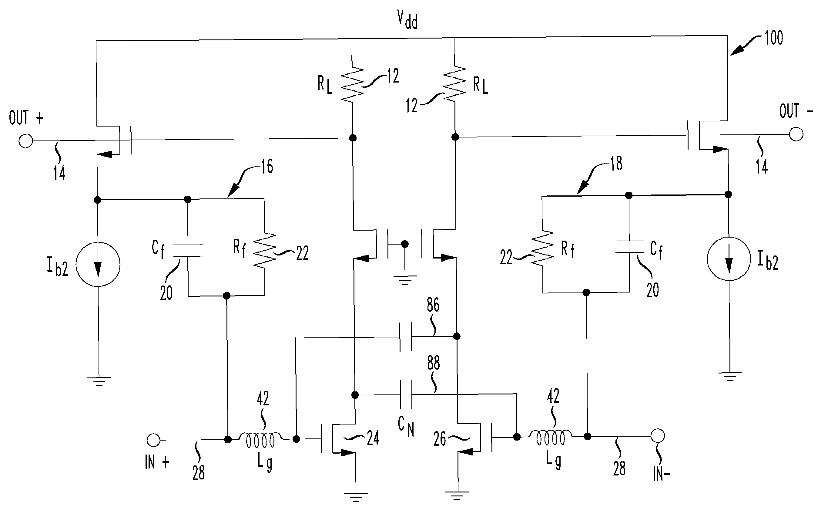
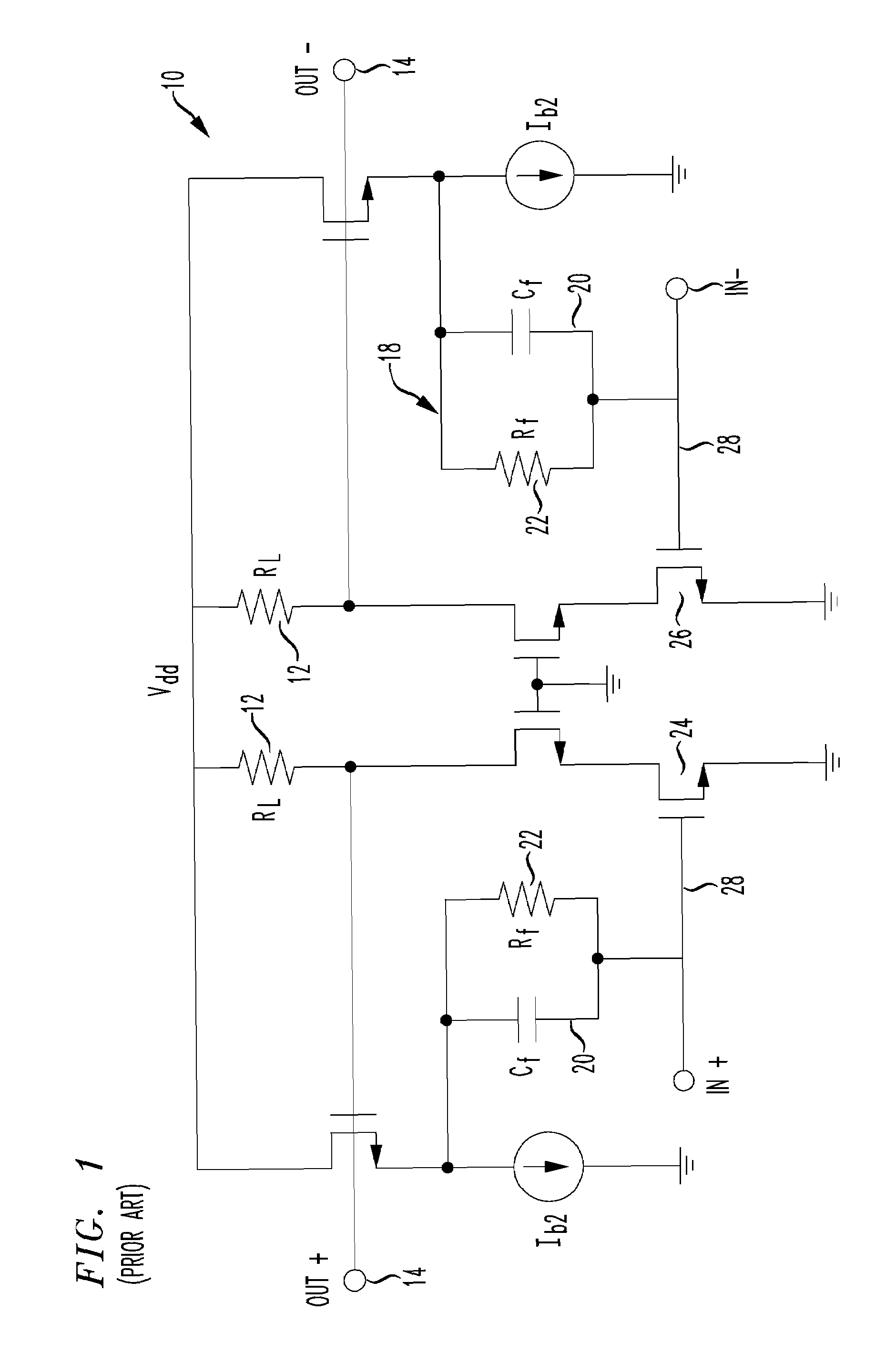
[0027]Referring now to FIG. 1, there is shown a schematic representation of a known resistive feedback amplifier circuit 10 for amplifying communications signals. In the amplifier circuit 10 a differential input signal could be applied to the differential input terminals 28. The differential input signal could thereby be applied to the input transistors 24, 26 for amplification. The input transistors 24, 26 were preferably provided with the feedback loops 16, 18, respectively. The feedback loops 16, 18 typically included the feedback resistors 22 for input matching purposes to thereby extend the bandwidth of the circuit 10. The feedback capacitors 20 could also be provided in the feedback loops 16, 18 in parallel with the feedback resistors 22 in order to further extend the bandwidth.

[0028]...


PUM


Abstract

A wideband amplifier having an amplifier input terminal and an amplifier output terminal includes at least one transistor coupled to the amplifier input terminal and an impedance element coupled between the amplifier input terminal and the amplifier output terminal. A feedback signal is transmitted between the amplifier output terminal and the amplifier input terminal by way of the impedance element wherein the feedback signal varies in accordance with changes in an impedance of the impedance element so as to peak a frequency response of the amplifier.

Description

BACKGROUND OF THE INVENTION[0001]1. Field of Invention[0002]This invention relates to in the field of amplification of high frequency communications signals.[0003]2. Description of Related Art[0004]Low Noise Amplifiers (LNAs) are well known in the art of amplifying weak signals in wireless communications systems. For example, LNAs were used in telephone systems including time division multiple access (TDMA) systems and code division multiple access (CDMA) systems. Since these systems were primarily directed to low data rate voice transmissions relatively narrow bandwidth amplifiers were adequate. For example, the frequency bandwidths that were amplified in these systems typically extended only to approximately 5 MHz.[0005]However, wide band LNAs are becoming increasingly important for a number of reasons. One reason is the fact that a new ultra-wide band (UWB) standard covering the range of approximately 3 GHz to 10 GHz has come into effect. See. The new standard was mainly directed...

Claims


Application Information

Patent Timeline
Patent Type & Authority Patents(United States)
IPC IPC(8): H03F3/45
CPCH03F1/08H03F1/26H03F1/42H03F3/45179H03F3/45188H03F2203/45554H03F2200/36H03F2200/372H03F2203/45481H03F2203/45526H03F2203/45532H03F2200/294
Inventor CHANG, TIENYUCHEN, JINGHONG
Owner BROADCOM INT PTE LTD
Why Eureka
Try Eureka