Basic cell design method for reducing the resistance of connection wiring between logic gates

a technology of logic gates and design methods, applied in the field of basic cell design methods, can solve the problems of increasing the chip size, high resistance of the connection between adjacent cells, and several layout methods, and achieve the effect of reducing the resistance of connection wiring

Active Publication Date: 2010-01-12
MICRON TECH INC
View PDF3 Cites 25 Cited by
  • Summary
  • Abstract
  • Description
  • Claims
  • Application Information

AI Technical Summary

Benefits of technology

[0020]It is an object of the present invention to provide a basic cell design method, a layout design method, a design device, and a program for reducing the resistance of connection wiring between logic gates in a logic circuit that is made up from a plurality of logic gates.
[0025]According to the present invention, first extended patterns are provided at the ends at which input wiring and output wiring extend in the longitudinal direction, whereby the areas in which connections are possible with cells that are adjacent in the longitudinal direction are broadened. In addition, second extended patterns of input wiring and output wiring are formed in the center of the cell, whereby the positions with respect to the longitudinal direction of the second extended patterns do not change despite 180° rotation of the cell. As a result, the connections between second extended patterns of cells that are adjacent in a direction that is perpendicular to the longitudinal direction are facilitated, and the degree of freedom of layout design is increased.
[0026]In the present invention, the patterns of input wiring and output wiring are formed as extended patterns that extend close to the cell boundaries, and as a result, in wiring connections with adjacent cells, the connection by wiring of the same layer as the input wiring and output wiring is facilitated. If input wiring and output wiring are formed by first-layer wiring, the wiring of second and subsequent layers need not be used for the wiring of inter-cell connections, and through-holes for connecting this wiring are thus not required. As a result, the present invention can suppress the increase in the resistance of inter-cell wiring that results from through-hole resistance. In addition, the provision of dummy patterns in vacant areas within cells prevents the provision of erroneous wiring in vacant areas.

Problems solved by technology

However, the above-described layout method has several problems as described below.
The first problem is the high resistance of the connections between adjacent cells.
This problem occurs because the connections between adjacent cells are realized by way of through-holes using the wiring material of second and subsequent layers, and the through-hole resistance, being greater than the wiring of second and subsequent layers, increases the resistance of inter-cell connections.
The second problem is the need for many wiring tracks of the second and subsequent layers and the consequent increase in chip size.
This problem occurs because the wiring material of second and subsequent layers must be used in the connections between adjacent cells.

Method used


Image

  • Basic cell design method for reducing the resistance of connection wiring between logic gates
  • Basic cell design method for reducing the resistance of connection wiring between logic gates
  • Basic cell design method for reducing the resistance of connection wiring between logic gates

Examples


first working example

[0042]Explanation first regards the design device used in the design method of a basic cell and layout in the present working example.

[0043]FIG. 4 is a block diagram showing an example of the configuration of the design device used in the present working example.

[0044]Design device 10 is an information processor such as a CAD tool, a personal computer, or a workstation. As shown in FIG. 4, design device 10 includes: memory unit 11 for storing logic circuit information and information such as design rules; control unit 12 for carrying out operations for the design of a basic cell and layout; output unit 13 for supplying the design results; and console unit 14 by which the designer enters instructions as input. Control unit 12 includes: CPU 16 for executing prescribed processes in accordance with programs; and memory 17 for storing programs. The design procedure of a basic cell is written in a program. The content of this design procedure of a basic cell will be explained later. Outpu...

second working example

[0071]Explanation next regards the configuration of a basic cell of the present working example with reference to the accompanying figures. As in the first working example, the logic gates are assumed to be inverters.

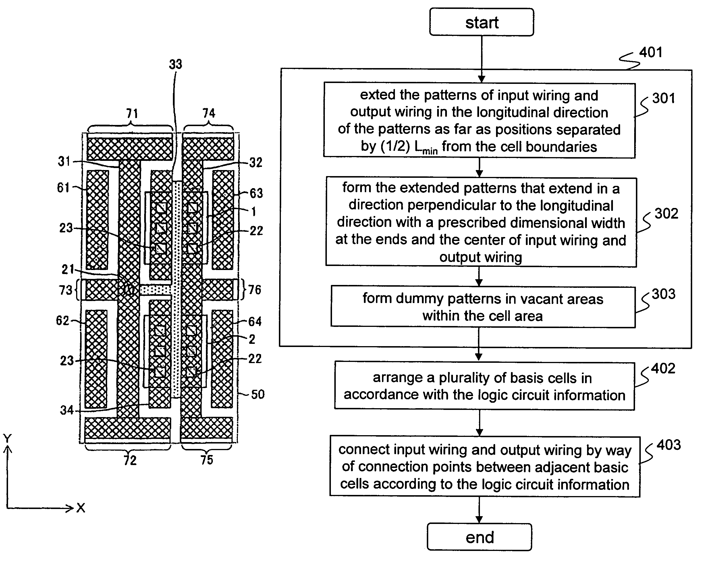
[0072]FIG. 8 shows the configuration of a basic cell in the present working example. In addition, the same reference numerals are used for configurations that are identical in the first working example, and detailed explanation of these configurations will be omitted. As in FIG. 5, the horizontal direction is the X-axis direction, and the vertical direction is the Y-axis direction in FIG. 8.

[0073]In the present working example, first-layer wiring 35 shown in FIG. 8 is input wiring Tin, and first-layer wiring 36 is output wiring Tout. As in the first working example, first-layer wiring 35 and first-layer wiring 36 have patterns that extend as far as positions separated by (½) Lmin from cell boundaries in the Y-axis direction. The difference with the first working example...

third working example

[0085]Explanation next regards the configuration of a basic cell of the present working example with reference to the accompanying figures. As in the first working example, logic gates are assumed to be inverters.

[0086]FIG. 11 shows the configuration of a basic cell in the present working example. The same reference numerals are conferred to configurations identical to those of the first working example, and detailed explanation of these configurations is omitted. As in FIG. 5, the horizontal direction is the X-axis direction, and the vertical direction is the Y-axis direction in FIG. 11.

[0087]In the present working example, first-layer wiring 37 shown in FIG. 11 is input wiring Tin, and first-layer wiring 38 is output wiring Tout. The difference between the present working example and the first and second working examples is the greatest possible reduction in the size of the patterns of input wiring Tin and output wiring Tout. First-layer wiring 37 is of a size that allows a patter...


PUM


Abstract

The basic cell design method of the present invention is a method for carrying out: extended pattern formation for extending the patterns of input wiring and output wiring in the longitudinal direction, forming first extended patterns that extend with a prescribed dimensional width in a direction perpendicular to the longitudinal direction at the ends of the extended patterns, and forming second extended patterns that extend with the prescribed dimensional width from the input wiring and the output wiring at the center of the cell in the longitudinal direction; and dummy pattern formation for subsequently arranging dummy patterns in vacant areas within the cell.

Description

[0001]This application is based upon and claims the benefit of priority from Japanese Patent Application No. 2005-316188 filed on 31 Oct. 2005, the content of which is incorporated by reference.BACKGROUND OF THE INVENTION[0002]1. Field of the Invention[0003]The present invention relates to a basic cell design method that is used in the design stage of a semiconductor devices such as gate arrays and standard cells, a layout design method for designing the layout of a logic circuit in which basic cells are combined, a design device for executing these methods, and a program for causing a computer to execute these methods.[0004]2. Description of the Related Art[0005]In designing the layout of a logic circuit, a step of arranging logic gates in accordance with logic circuit information that includes information on the number of logic gates and the connection relations between these gates and a step of connecting the logic gates by wiring are carried out in succession. The logic gates th...

Claims


Application Information

Patent Timeline
Patent Type & Authority Patents(United States)
IPC IPC(8): G06F17/50
CPCG06F17/5068G06F30/39
Inventor HARUKI, TADASHI
Owner MICRON TECH INC
Why Eureka
Try Eureka