Semiconductor device with two overlapping diffusion layers held at floating voltage for improving withstand voltage
a technology of diffusion layer and semiconductor, applied in the direction of semiconductor devices, basic electric elements, electrical equipment, etc., can solve the problems of increasing the on-state resistance value, difficult to achieve desired current, and difficult to achieve desired withstand voltage characteristics
- Summary
- Abstract
- Description
- Claims
- Application Information
AI Technical Summary
Benefits of technology
Problems solved by technology
Method used
Image

Examples
Embodiment Construction
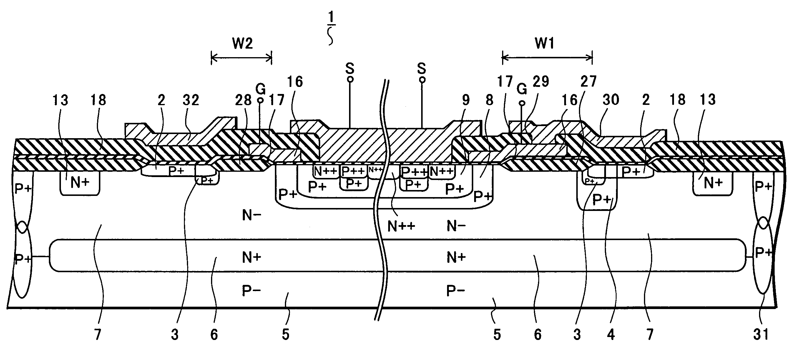
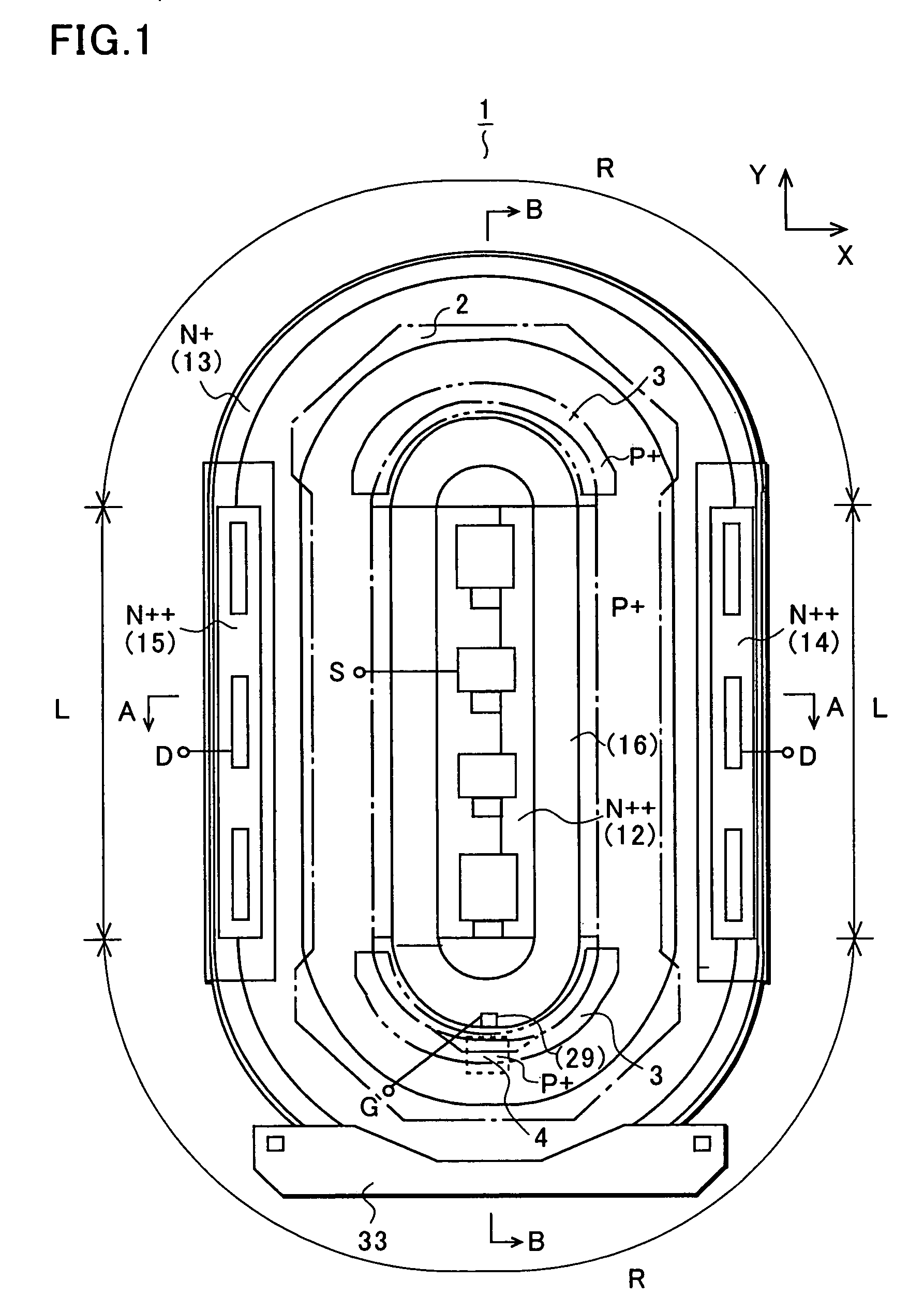
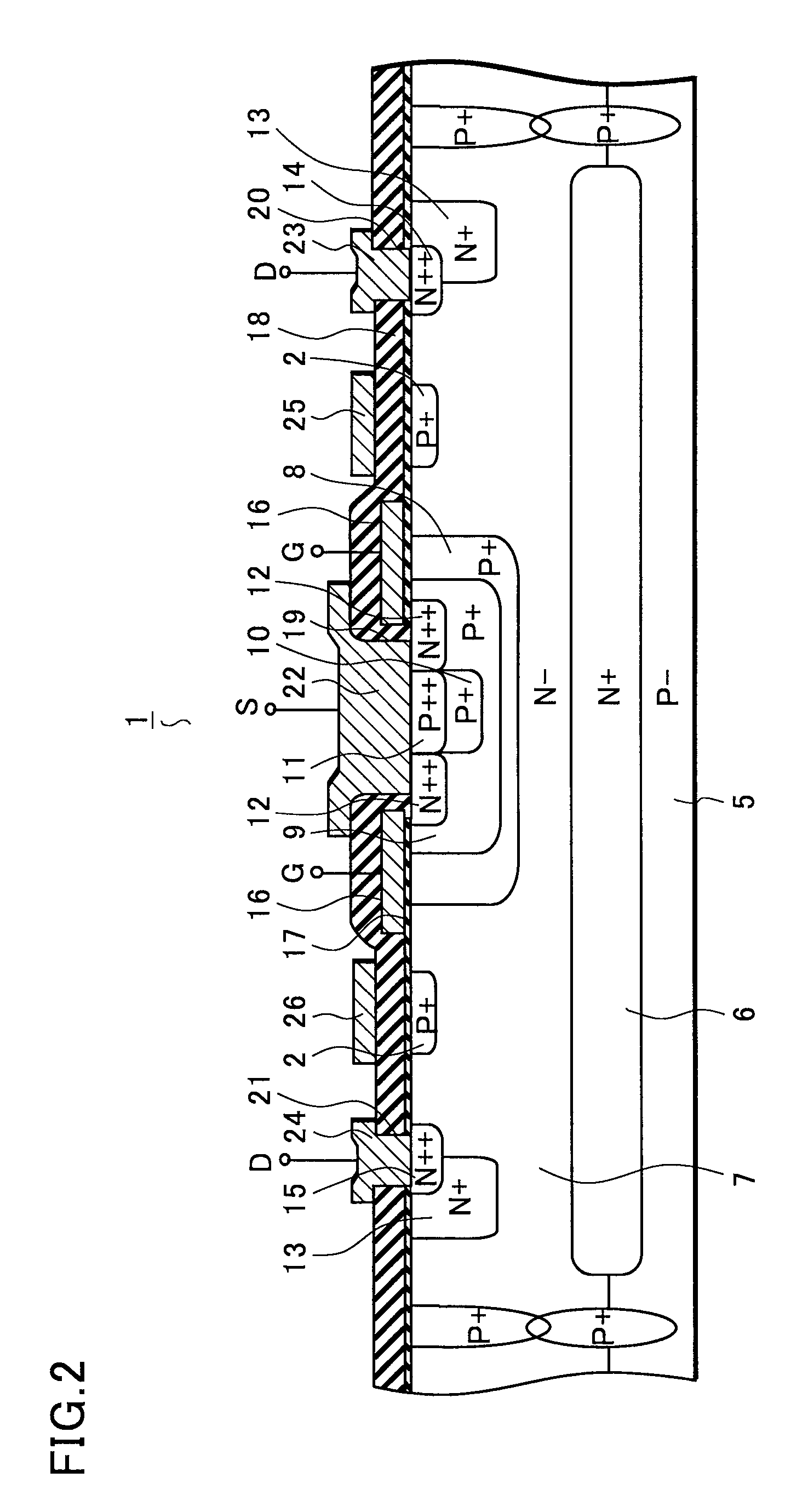
[0018]A semiconductor device according to one embodiment of the present invention will be described in detail below with reference to FIGS. 1 to 5B. FIG. 1 is a plan view for explaining an N channel type MOS transistor according to the embodiment. FIG. 2 is a cross-sectional view taken along the line A-A of FIG. 1, for explaining the N channel type MOS transistor according to the embodiment. FIG. 3 is a cross-sectional view taken along the line B-B of FIG. 1, for explaining the N channel type MOS transistor according to the embodiment. FIG. 4A is a view for explaining the potential distribution in a reverse state of the N channel type MOS transistor according to the embodiment. FIG. 4B is a view for explaining an impact ionization region of the N channel type MOS transistor according to the embodiment. FIG. 5A is a view for explaining the potential distribution in a reverse bias state of the N channel type MOS transistor according to the embodiment. FIG. 5B is a view for explaining ...
PUM
 Abstract
Description
Claims
Application Information