Semiconductor package having embedded passive elements and method for manufacturing the same

a passive element and semiconductor technology, applied in the direction of semiconductor devices, semiconductor/solid-state device details, electrical apparatus, etc., can solve the problems of impeding the miniaturization and slimness of electronic appliances, limiting the size and thickness of printed circuit boards which are finally arranged in electronic appliances, and limiting the electrical performance of electronic appliances

Active Publication Date: 2010-01-26
SK HYNIX INC
View PDF9 Cites 2 Cited by
  • Summary
  • Abstract
  • Description
  • Claims
  • Application Information

AI Technical Summary

Benefits of technology

[0008]Embodiments of the present invention are directed to a semiconductor package, which eliminates the factors impeding the miniaturization and slimness of an electronic appliance, and a method for manufacturing the same.
[0009]Further, embodiments of the present invention are directed to a semiconductor package which minimizes electrical connection lengths between a semiconductor chip and passive elements, thereby improving the electrical performance of the electrical appliance, and a method for manufacturing the same.
[0010]Also, embodiments of the present invention are directed to a semiconductor package which can prevent damage to a semiconductor chip, even having a wafer level package structure, and a method for manufacturing the same.

Problems solved by technology

However, in spite of efforts to decrease the size and the thickness of a semiconductor package to attain miniaturization of the semiconductor package, due to the presence of passive elements such as a resistor, an inductor and a capacitor, which are mounted along with the semiconductor package, limitations necessarily exist in decreasing the size and the thickness of the printed circuit board which is finally arranged in an electronic appliance, and this serves as a factor impeding the miniaturization and the slimness of the electronic appliance.
As a consequence, since the inductance component increases, limitations exist in improving the electrical performance of the electronic appliance.
In addition, in the case of a wafer level package which is a kind of chip-size package, as the rear surface of a semiconductor chip is exposed to the outside, the semiconductor chip is likely to be damaged by an external shock and mis-operate, whereby it is difficult to ensure the reliability of an end product.

Method used


Image

  • Semiconductor package having embedded passive elements and method for manufacturing the same
  • Semiconductor package having embedded passive elements and method for manufacturing the same
  • Semiconductor package having embedded passive elements and method for manufacturing the same

Examples


Embodiment Construction

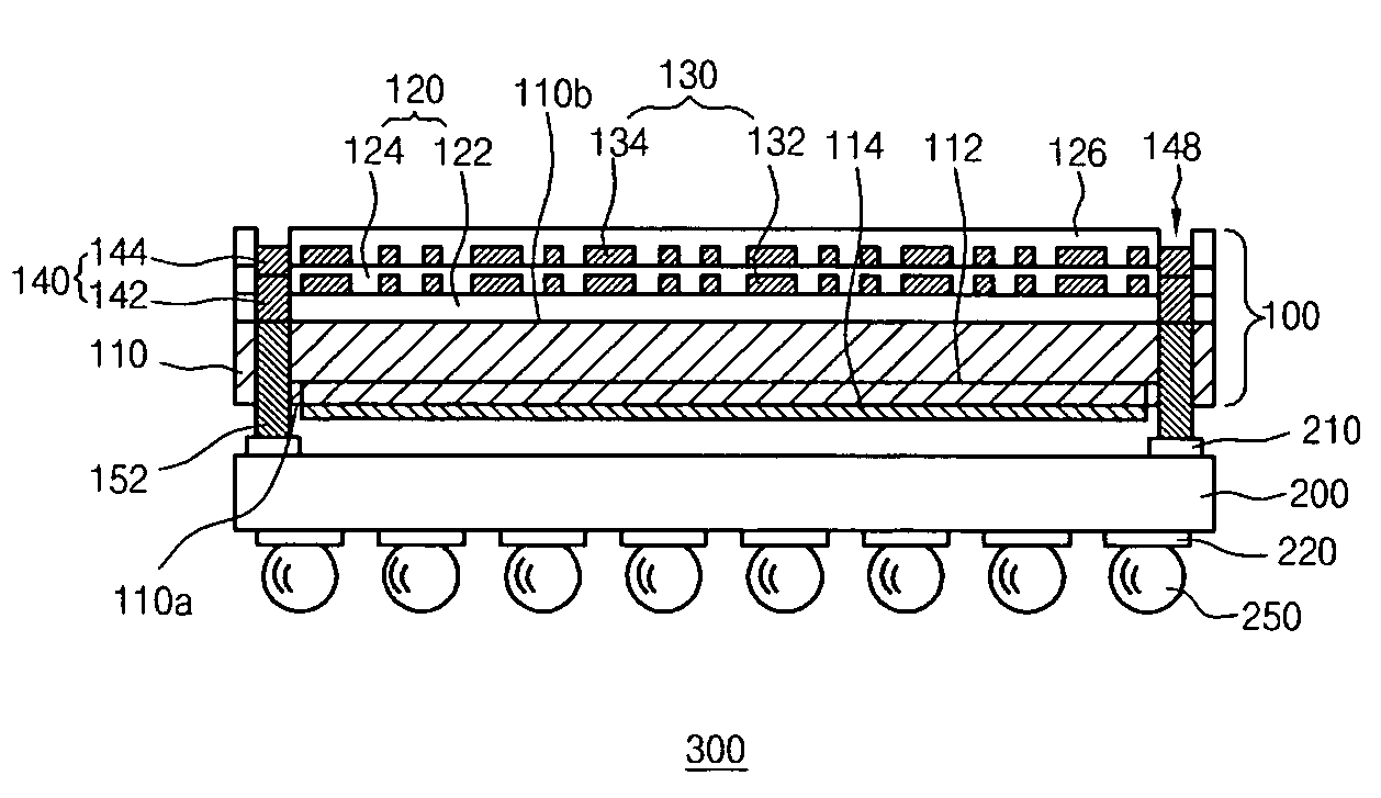
[0030]A preferred embodiment of the present invention is directed to a semiconductor package in which passive elements, including a resistor, an inductor, and a capacitor, are embedded. That is to say, in an embodiment of the present invention, by forming the passive elements, including a resistor, an inductor and a capacitor, on the rear surface of a semiconductor chip, a semiconductor chip unit is configured, and by mounting the semiconductor chip unit to a base substrate, a semiconductor package is configured.

[0031]Therefore, in an embodiment of the present invention, since the passive elements are installed on the rear surface of the semiconductor chip, in a printed circuit board, a separate area for mounting the passive elements is not required. Accordingly, in the semiconductor package according to an embodiment of the present invention, through the miniaturization of the package, the miniaturization and slimming of an electronic appliance can be attained.

[0032]Also, the semic...


PUM


Abstract

A semiconductor package includes a base substrate on which a semiconductor chip is placed so that a first surface thereof faces the base substrate. A circuit section is formed adjacent to the first surface. An insulation layer is formed on a second surface of the semiconductor chip which faces away from the first surface. Passive elements are formed on the insulation layer. Via patterns are formed to pass through the insulation layer and are connected to the passive elements. Via wirings are formed to pass through the semiconductor chip and connected to the circuit section, the via patterns and the base substrate. Outside connection terminals are attached to a first surface of the base substrate, which face away from a second surface of the base substrate on which the semiconductor chip is placed.

Description

CROSS-REFERENCE TO RELATED APPLICATIONS[0001]The present application claims priority to Korean patent application number 10-2006-0059827 filed on Jun. 29, 2006, which is incorporated herein by reference in its entirety.BACKGROUND OF THE INVENTION[0002]The present invention relates to a semiconductor package, and more particularly, to a semiconductor package in which passive elements are embedded, and a method for manufacturing the same.[0003]In the semiconductor industry, a semiconductor package is a structure in which a semiconductor chip, having a fine circuit pattern designed therein, is molded by resin, ceramic, etc. so that the semiconductor chip can be protected from the surrounding environment and can be mounted to an electronic appliance. Rather than packaging a semiconductor chip in order to simply protect the semiconductor chip and then mounting the semiconductor chip to an electronic appliance, a semiconductor chip may be packaged in order to improve the performance and q...

Claims


Application Information

Patent Timeline
Patent Type & Authority Patents(United States)
IPC IPC(8): H01L23/58H01L21/8222
CPCH01L21/6835H01L21/76898H01L23/50H01L23/5223H01L24/12H01L25/16H01L25/50H01L2924/00014H01L2224/13025H01L2224/05573H01L2221/68372H01L2224/13009H01L2224/13099H01L2224/16H01L2225/06513H01L2225/06517H01L2225/06541H01L2924/01015H01L2924/01033H01L2924/01078H01L2924/15311H01L2924/19041H01L2924/19042H01L2924/19043H01L2924/30105H01L2924/30107H01L2924/01006H01L2924/01047H01L2924/014H01L2924/181H01L2924/00H01L2224/05599H01L2224/0554H01L2224/0555H01L2224/0556H01L23/12H01L27/04
Inventor YANG, SEUNG TAEK
Owner SK HYNIX INC
Why Eureka
Try Eureka