Semiconductor device and method of manufacturing the same

a semiconductor device and semiconductor technology, applied in semiconductor devices, capacitors, electrical devices, etc., can solve the problems of increasing the chip size affecting the miniaturization of the semiconductor device, and not maintaining the reliability of the capacitor element, so as to achieve the effect of improving the performance of the semiconductor devi

Active Publication Date: 2020-09-17
RENESAS ELECTRONICS CORP
View PDF0 Cites 1 Cited by
  • Summary
  • Abstract
  • Description
  • Claims
  • Application Information

AI Technical Summary

Benefits of technology

[0014]According to one embodiment, the performa

Problems solved by technology

In order to manufacture a large-capacity semiconductor device and improve the performance of the semiconductor device, it is only necessary to increase the number of capacitive elements formed in the semiconductor substrate, but this increases the chip size of the semiconductor device and hinders the miniaturization of the semiconductor device.
As another method, although the value of the unit capacitance can be increased by reducing the thickness of the capa

Method used


Image

  • Semiconductor device and method of manufacturing the same
  • Semiconductor device and method of manufacturing the same
  • Semiconductor device and method of manufacturing the same

Examples


embodiment 1

[0036]The semiconductor device of the present embodiment will be described below by referring to the drawings. The semiconductor device of the present embodiment has a capacitor element using an isolation-layer PiSO which is a p-type impurity region in an element isolation region 1A in which no semiconductor element such as a capacitor element or a transistor is conventionally formed.

[0037]

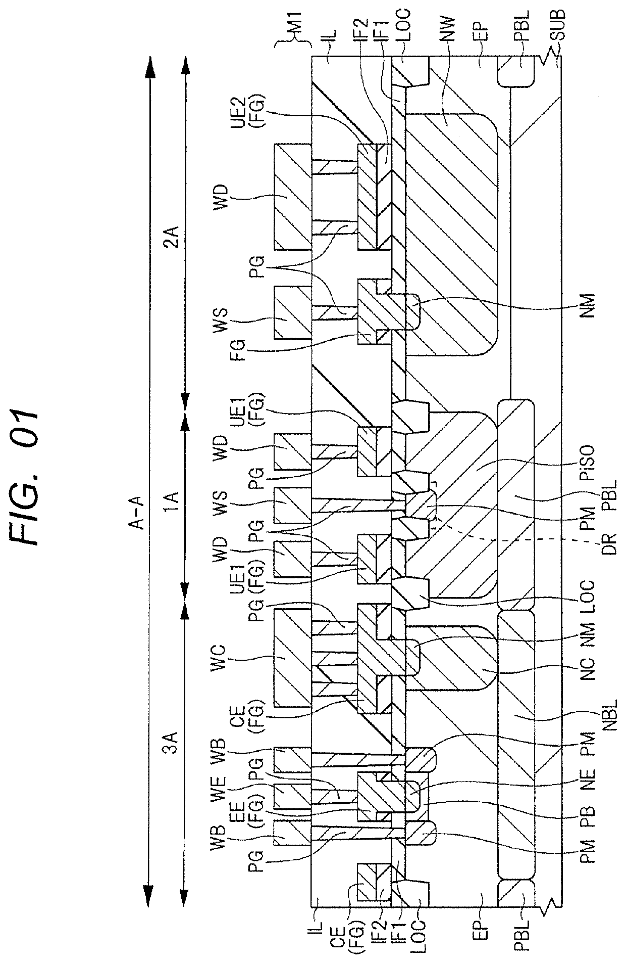
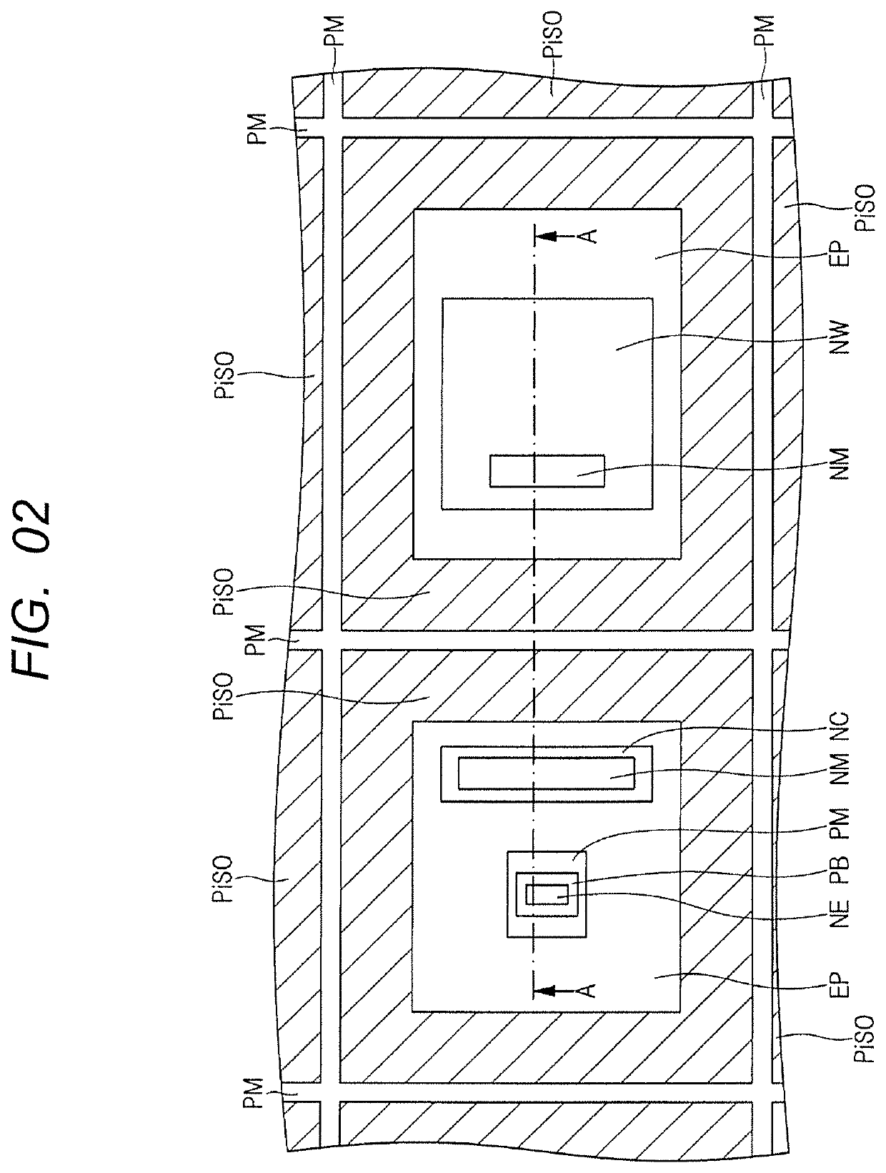
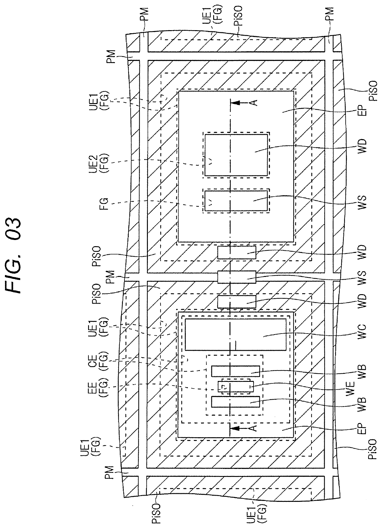
[0038]Hereinafter, the structure of the semiconductor device of the present embodiment will be described in detail with reference to FIGS. 1 to 3. FIG. 1 shows a cross-sectional view of the semiconductor device and is a cross-sectional view along the line A-A shown in FIGS. 2 and 3. FIG. 2 shows the planar structures of the semiconductor device, and shows the relative positions of the impurity regions formed in the vicinity of the surfaces of the n-type semiconductor layers shown in FIG. 1. FIG. 3 shows the planar structures of the semiconductor device, and shows the relative positions of the elec...

embodiment 2

[0114]Hereinafter, the semiconductor device of the embodiment 2 will be described with reference to FIG. 17. Hereinafter, differences from the semiconductor device of the embodiment 1 will be mainly described.

[0115]In embodiment 1, the side surface SS2 of the upper electrode UE1 is provided on the inner side of the isolation layer PiSO from the interface between the isolation layer PiSO and the semiconductor layer EP, and is provided at a position equal to or less than (3 / 4)×the distance LA from the defective area DR.

[0116]In the embodiment 2, the length of the upper electrode UE1 is increased, and the side surface SS2 of the upper electrode UE1 is provided at a position larger than (3 / 4)×the distance LA from the defect region DR, and in FIG. 17, it is provided at a position at a distance LA from the defect region DR. That is, the side surface SS2 of the upper electrode UE1 is provided on the interface between the isolation layer PiSO and the semiconductor layer EP, which correspond...

embodiment 3

[0120]The semiconductor device of the embodiment 3 will be described below with reference to FIG. 18. Hereinafter, differences from the semiconductor device of the embodiment 1 will be mainly described.

[0121]In the embodiment 1, the upper electrodes UE1 are not provided immediately above the defective regions DR in order to prevent the film quality of the capacitor insulating film from deteriorating in the region 1A.

[0122]In the embodiment 3, as shown in FIG. 18, the upper electrodes UE1, the insulating films IF2, and the insulating films IF1 are also formed directly on the defective regions DR (diffusion regions PM) at the portions where the plugs PG connected to the reference potential wiring WS are not formed, and the capacitive elements are formed on the defective regions DR (diffusion regions PM). Here, since the separation layer PiSO in FIG. 18 is integrally connected to the separation layer PiSO of the embodiment 1 or the embodiment 2, the separation layer PiSO in the embodim...


PUM


Abstract

A semiconductor device includes a semiconductor substrate SUB, a semiconductor layer EP formed on the semiconductor substrate SUB, a buried layer PBL formed between the semiconductor layer EP and the semiconductor substrate SUB, an isolation layer PiSO formed in the semiconductor layer EP so as to be in contact with the buried layer PBL, and a conductive film FG formed over the isolation layer PiSO via an insulating film IF, whereby a first capacitive element including the conductive film FG as an upper electrode, the insulating film IF as a capacitive insulating film, and the isolation layer PiSO as a lower electrode, is formed over the semiconductor substrate SUB.

Description

CROSS-REFERENCE TO RELATED APPLICATIONS[0001]The disclosure of Japanese Patent Application No. 2019-044346 filed on Mar. 12, 2019 including the specification, drawings and abstract is incorporated herein by reference in its entirety.BACKGROUND OF THE INVENTION[0002]The present invention relates to a semiconductor device and a manufacturing method thereof, and in particular, the present invention can be suitably applied to a semiconductor device having a device isolation region formed of an impurity region.[0003]In recent years, a semiconductor device (semiconductor chip) for use in a vehicle is required to have a performance that operates normally even when subjected to electromagnetic interference such as EMC (Electro Magnetic Compatibility) resistance. As a method for improving the resistance to EMCs, by providing a capacitance between the power supply potential (Vdd) and the reference potential (Vss, GND), it is possible to attenuate noises (electromagnetic interference) that hav...

Claims


Application Information

Patent Timeline
IPC IPC(8): H01L27/01H01L49/02H01L21/265H01L21/225H01L21/324H01L21/70
CPCH01L21/324H01L28/60H01L21/2253H01L27/013H01L21/26513H01L21/705H01L29/94H01L27/0658H01L21/761H01L27/0733H01L27/0727
Inventor KODAMA, EISUKE
Owner RENESAS ELECTRONICS CORP
Why Eureka
Try Eureka