Semiconductor device and its production method

a technology of semiconductors and semiconductors, applied in the direction of semiconductor devices, electrical devices, transistors, etc., can solve the problems of undesirable segregation, achieve the effect of sacrificing device characteristics, and reducing the size of mos

Inactive Publication Date: 2004-08-24
HITACHI LTD
View PDF4 Cites 2 Cited by
  • Summary
  • Abstract
  • Description
  • Claims
  • Application Information

AI Technical Summary

Benefits of technology

It is an object of the present invention to provide a method for forming a delta doping layer which prevents punch-through hindering miniaturization of MOSFET without sacrificing the device characteristics in an accurate, stable and inexpensive manner.
According to the present invention, prevention of punch-through is accomplished by introducing dopant atoms into the semiconductor substrate through ion implantation and subsequently causing the dopant atoms to segregate in the surface, with the resulting surface layer functioning as the delta doping layer. Ion implantation offers a technical advantage of permitting one to accurately specify the doping position and accurately control the doping amount. It also offers an economical advantage of requiring no additional investment in production facilities. Incidentally, the term "segregation" denotes a phenomenon that impurity atoms distribute themselves in the semiconductor substrate such that their concentration is higher in the surface than in the inside.

Problems solved by technology

Such segregation has been regarded as undesirable from the standpoint of keeping the doping amount as high as possible.

Method used


Image

  • Semiconductor device and its production method
  • Semiconductor device and its production method
  • Semiconductor device and its production method

Examples


example 2

This example demonstrates, with reference to FIGS. 6A to 6D, production of a PMOS in which the n-type delta doping layer functions as the punch-through stopper and the p-type delta doping layers functions as the extensions of the source and the drain.

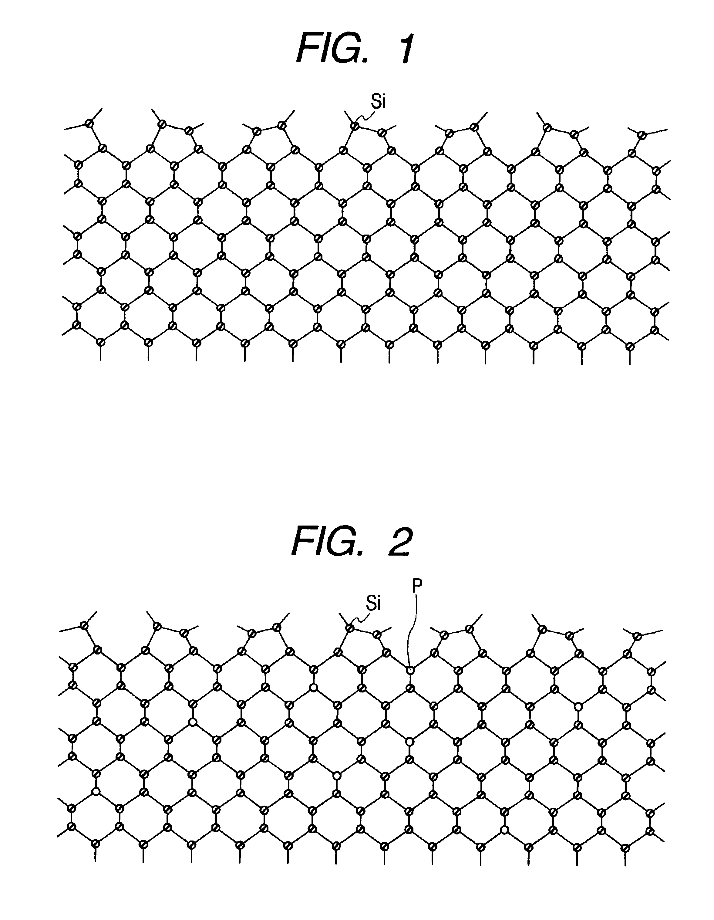
In the first step shown in FIG. 6A, the substrate prepared in the third step (FIG. 5C) of Example 1 is doped with boron atoms by ion implantation into its surface. This ion implantation forms a p-type doped region 22 (about 0.3 .mu.m thick) with a concentration of about 10.sup.17 / cm.sup.3.

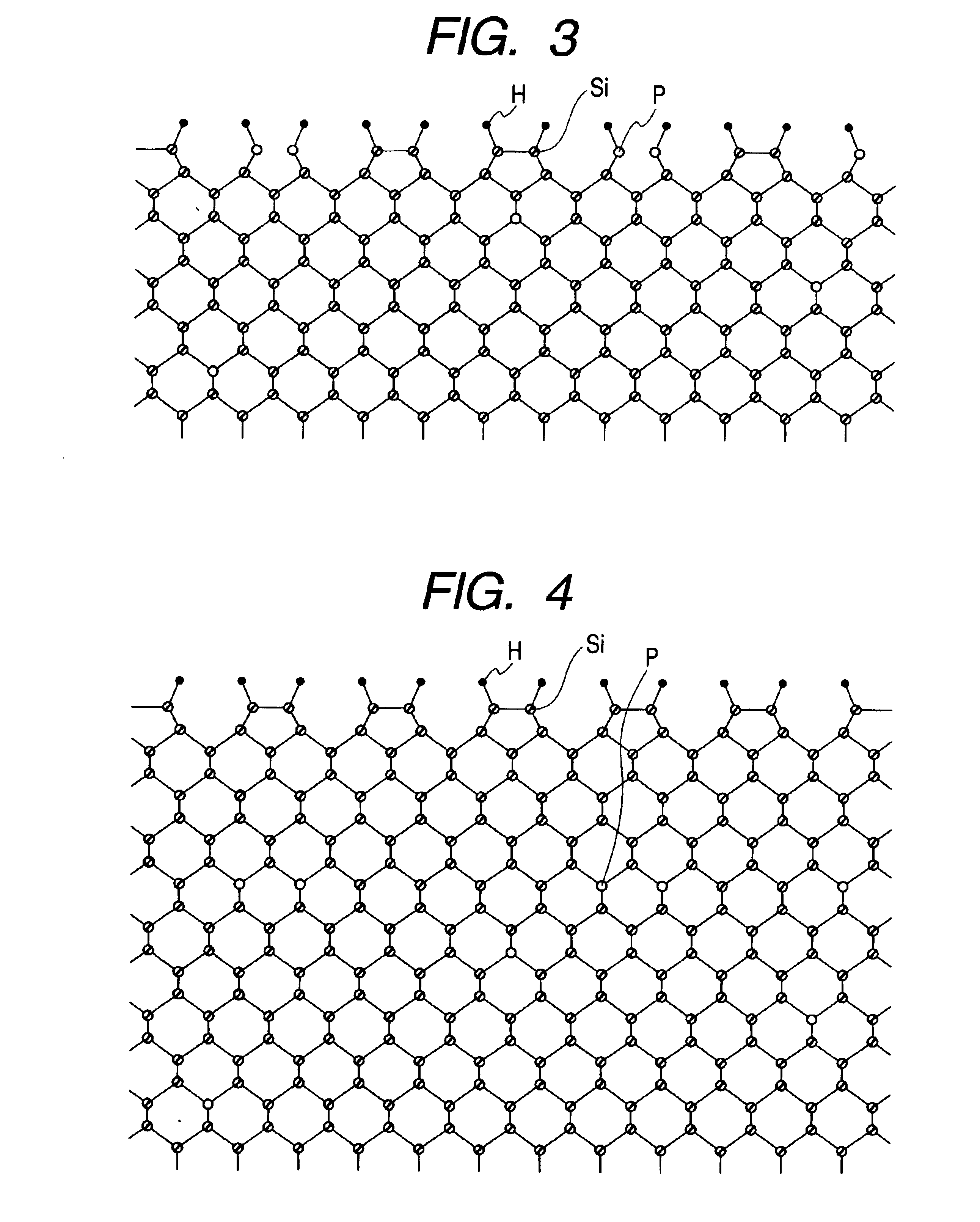
In the second step shown in FIG. 6B, the surface of the substrate undergoes hydrogen termination in the same way as mentioned in Example 1. This hydrogen termination causes boron atoms to segregate in the surface, so that a p-type delta doping layer 23 is formed under the surface hydrogen atomic layer. The p-type delta doping layer 23 has a thickness of one atomic layer and a concentration of about 10.sup.18 / cm.sup.3.

In the third step shown in FIG. 6...

example 3

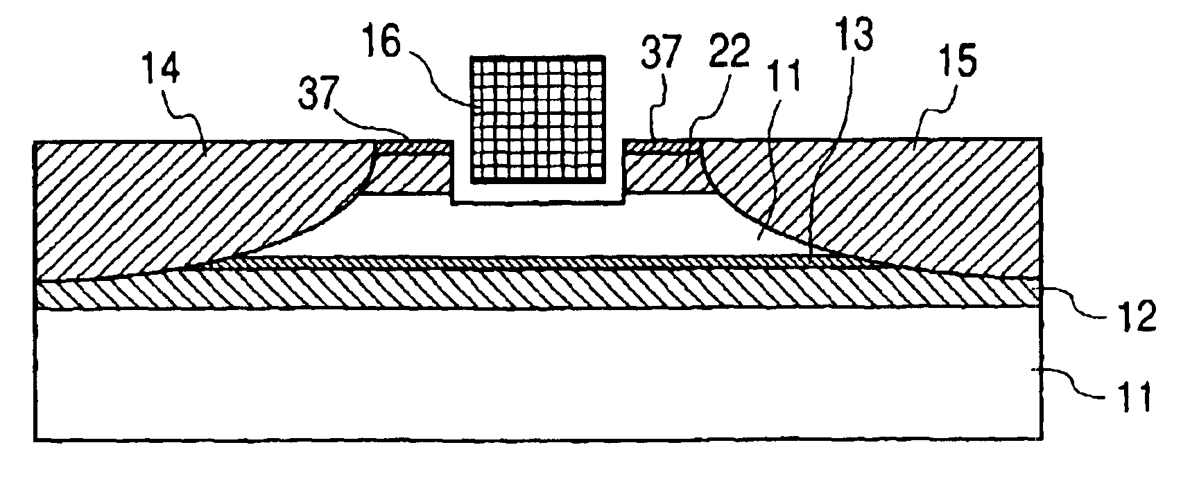
This example demonstrates, with reference to FIGS. 7A to 7D, production of a CMOS which is a combination of a PMOS and an NMOS, the former having an n-type delta doping layer as the punch-through stopper and the latter having a p-type delta doping layer as the punch-through stopper.

In the first step shown in FIG. 7A, an oxide film 32 for element separation is formed in the silicon substrate 11 in the usual way. The clean surface of silicon is exposed. Phosphorus atoms are implanted into the surface at the right side of the oxide film 32. This implantation forms an n-type doped region 12 which is about 0.3 .mu.m thick and has a concentration of about 10.sup.17 / cm.sup.3. Then, boron atoms are implanted into the surface at the left side of the oxide film 32. This implantation forms a p-type doped region 22 which is about 0.3 .mu.m thick and has a concentration of about 10.sup.17 / cm.sup.3. FIGS. 7A to 7D show only one each of adjacent PMOS and NMOS for simplicity. In an actual semicon...

example 4

This example demonstrates, with reference to FIGS. 8A to 8C and FIG. 9, production of a semiconductor substrate having PMOSs on both sides thereof, each PMOS having an n-type delta doping layer as the punch-through stopper. The PMOSs are formed in the same way as explained in Example 1. FIGS. 8A to 8C correspond to FIGS. 5A to 5C, and FIG. 9 corresponds to FIG. 5E.

In the first step shown in FIG. 8A, the silicon substrate 11 is doped with phosphorus atoms by ion implantation into both sides thereof. This ion implantation forms an n-type doped region 12 (about 0.3 .mu.m thick) with a concentration of about 10.sup.17 / cm.sup.3 on both sides.

In the second step shown in FIG. 8B, the both surfaces of the substrate undergo hydrogen termination in the same way as mentioned in Example 1. This hydrogen termination causes phosphorus atoms to segregate to the surface, so that an n-type delta doping layer 13 is formed under the surface hydrogen atomic layer. The n-type delta doping layer 13 has ...


PUM


Abstract

A method for producing a semiconductor device which comprises causing a dopant present in a semiconductor substrate to segregate in the surface of said semiconductor substrate, thereby forming a thin layer which has a higher dopant concentration than said substrate. The thin layer formed by segregation prevents punch-through which occurs as the result of miniaturization of MOSFET. This method permits economical delta doping without sacrificing the device characteristics.

Description

1. Field of the InventionThe present invention relates to a semiconductor device and a method for production thereof. More particularly, the present invention relates to a technology to permit miniaturization of semiconductor integrated circuits by providing the substrate with a dopant-rich thin layer buried therein.2. Description of the Related ArtSilicon integrated circuits owe their high integration level and high speed to miniaturization of fabrication dimensions. However, in the case of MOSFET (metal oxide semiconductor field effect transistor), miniaturization poses a problem with punch-through, which is a phenomenon that current flows from the drain to the source due to a short circuit between them. One way to address this problem was by increasing doping concentration of the region between the source and the drain whose doping type is opposite to that of the source and the drain. This conventional approach, however, is not satisfactory when miniaturization progresses to such...

Claims


Application Information

Patent Timeline
Patent Type & Authority Patents(United States)
IPC IPC(8): H01L21/336H01L29/02H01L21/02H01L21/30H01L21/70H01L29/78H01L29/10H01L21/8238H01L29/66H01L21/22H01L21/225H01L21/8234H01L27/088H01L27/092
CPCH01L21/3003H01L21/823807H01L29/1083H01L29/66537H01L29/66545H01L29/66621H01L29/7834H01L21/20
Inventor SUWA, YUJIHASHIZUME, TOMIHIROYAMAGUCHI, KENFUJIMORI, MASAAKI
Owner HITACHI LTD
Why Eureka
Try Eureka