Silicon-based optical modulator for analog applications

an optical modulator and silicon-based technology, applied in the field of optical modulators, can solve the problems of unsuitable for many current applications which require high density integration, and a high degree of linearity, and achieve the effect of reducing the size and cost of the complete system

Active Publication Date: 2010-02-02
CISCO TECH INC
View PDF32 Cites 22 Cited by
  • Summary
  • Abstract
  • Description
  • Claims
  • Application Information

AI Technical Summary

Benefits of technology

[0008]In one embodiment of the present invention, a single SISCAP device may be used, disposed along one arm of the MZI structure. Preferably, a pair of SISCAP devices are used in a balanced configuration, disposed in parallel along each arm. The balanced arrangement is preferred inasmuch as it allows for adjustment in biasing conditions to overcome inherent fabrication differences between the waveguides. The ability to configure this arrangement in a common mode embodiment allows for differential signaling and reduced voltage levels to be used to obtain the same results as compared to the “single-sided” embodiment.
[0011]It is an advantage of the arrangement of the present invention that the use of silicon-based SISCAP optical devices allows for the formation of an analog optical modulator which is orders of magnitude smaller in overall dimensions than the above-described prior art LiNbO3 devices. In particular, a SISCAP analog optical modulator of the present invention requires a length on the order of about 100 μm (compared with 75 mm for the prior art) and a voltage sensitivity V, of about 0.8 V (compared with a V, of the prior art on the order of 3.0 V).
[0012]Importantly, the use of a silicon-based modulator allows for associated optical components (such as, for example, optical filters and photodetectors) and associated electrical components (such as, for example, transimpedance amplifiers and input signal filters) to be directly integrated within the same silicon substrate as the modulator, further reducing the size and cost of the complete system. Indeed, the use of a silicon-based analog optical modulator in accordance with the present invention allows for multiple modulators, disposed in various types of array configurations, to all be integrated within a single silicon substrate—along with associated optical and electrical components. The ability to form a monolithic array of optical modulators is considered a significant advance, particularly in light of various applications which require a small form factor for these components.

Problems solved by technology

LiNbO3-based devices are relatively large (having a length on the order of, for example, 75 mm), which makes them ill-suited for many current applications which require high density integration, as well as a high degree of linearity.
Moreover, the power dissipation associated with conventional LiNbO3 modulators renders them essentially useless for applications where available power or power consumption is a concern.

Method used


Image

  • Silicon-based optical modulator for analog applications
  • Silicon-based optical modulator for analog applications
  • Silicon-based optical modulator for analog applications

Examples


Embodiment Construction

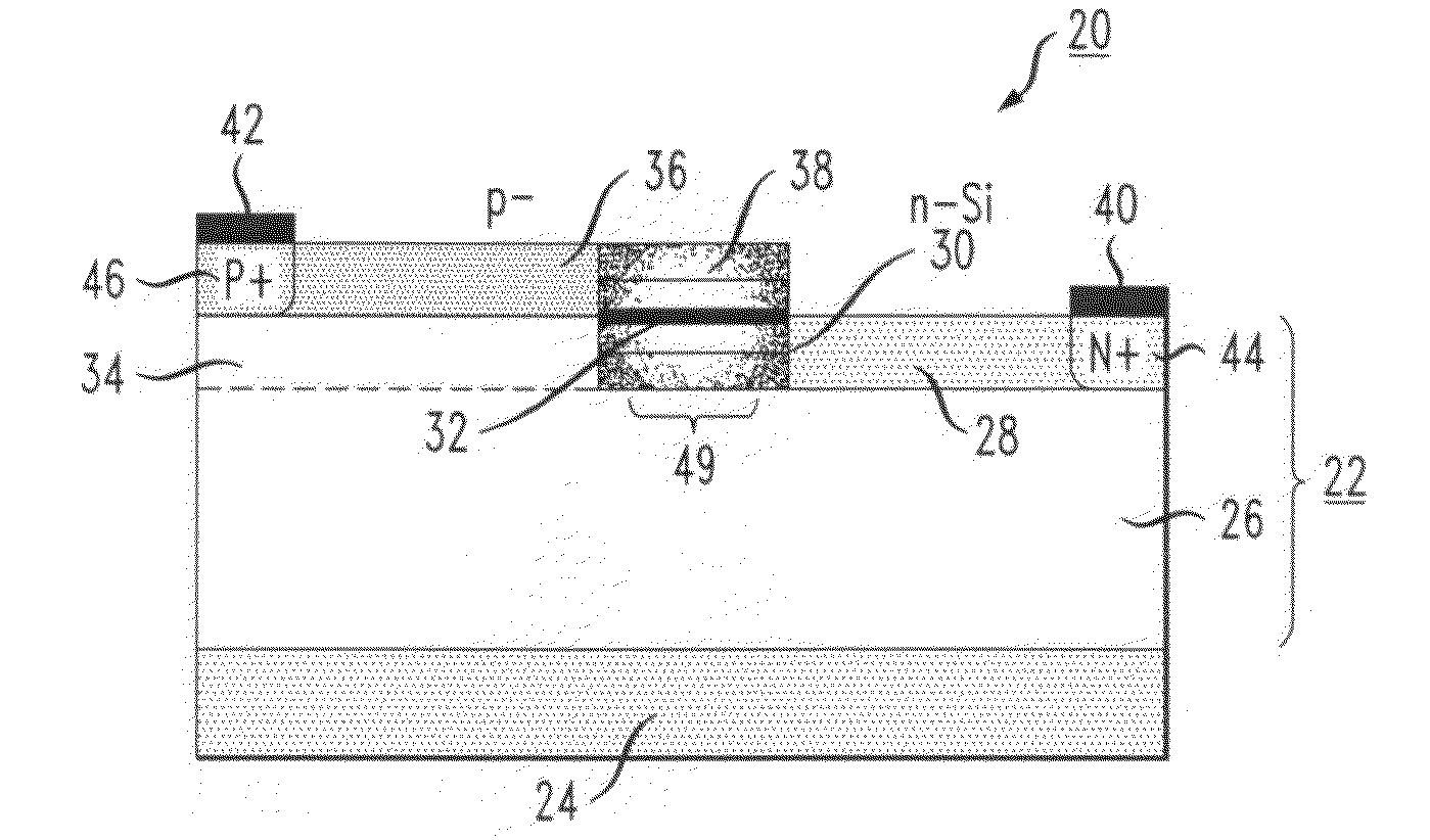
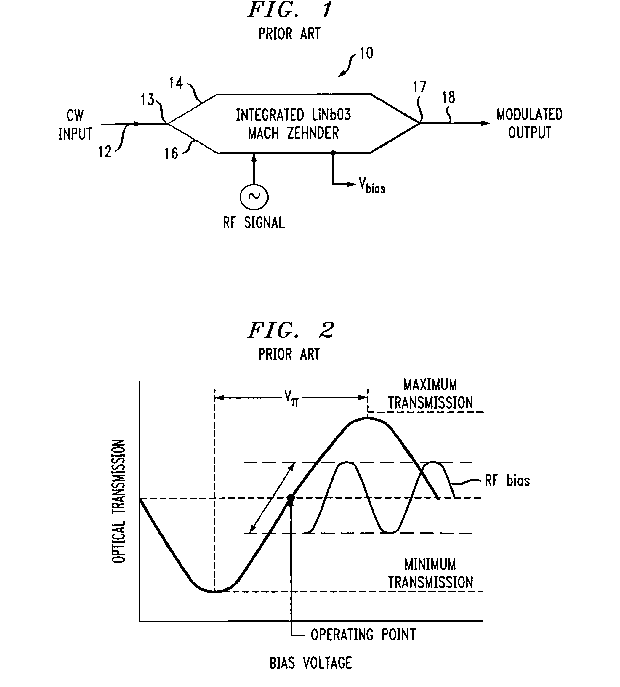
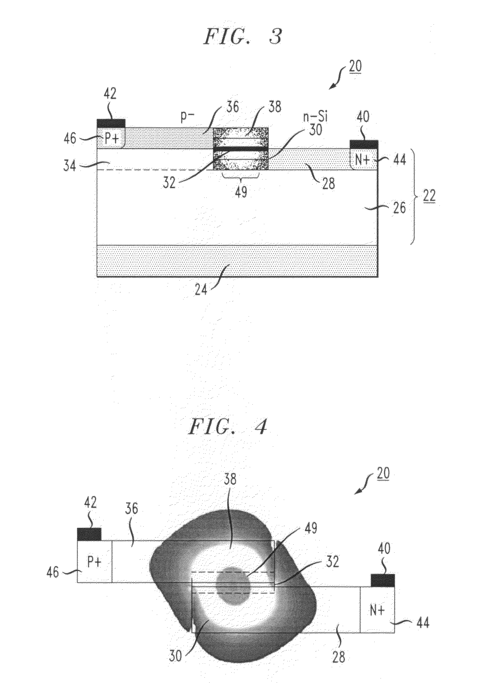
[0030]FIG. 1 illustrates a conventional prior art method of transmitting information on an optical carrier. A continuous wave (CW) optical input is coupled into input waveguide 12 of a Mach-Zehnder interferometer (MZI 10) and is then split at an input Y-branch 13 to thereafter propagate along a pair of parallel optical waveguide arms 14 and 16. Parallel optical waveguide arms 14, 16 form two phase modulators which operate in the well-known push-pull manner. In this prior art arrangement, phase modulation is made possible due to the electro-optic properties of the LiNbO3 material used for the modulator. Optical signals from the upper waveguide path 14 and lower waveguide path 16 are recombined at the output Y-branch 17 and then propagate along output waveguide 18. If the optical beams from the two paths 14, 16 arrive in phase, light will be guided out of the MZI 10, and vice-versa (that is, if the two signals arrive 180° out of phase—cancelling each other—no light will be coupled int...


PUM

PropertyMeasurementUnit
lengthaaaaaaaaaa
voltage sensitivityaaaaaaaaaa

Abstract

A silicon-insulator-silicon capacitive (SISCAP) optical modulator is configured to provide analog operation for applications which previously required the use of relatively large, power-consuming and expensive lithium niobate devices. An MZI-based SISCAP modulator (preferably a balanced arrangement with a SISCAP device on each arm) is responsive to an incoming high frequency electrical signal and is biased in a region where the capacitance of the device is essentially constant and the transform function of the MZI is linear.

Description

CROSS-REFERENCE TO RELATED APPLICATIONS[0001]This application claims the benefit of U.S. Provisional Application Nos. 60 / 999,784, filed Oct. 19, 2007 and 61 / 188,975, filed Aug. 13, 2008.TECHNICAL FIELD[0002]The present invention relates to an optical modulator for use with analog input signals (RF electrical input signals, for example) and, more particularly, to a silicon-based, relatively small analog optical modulator biased to operate in a linear region in which the analog input signal will be accurately replicated as the modulator's optical output signal.BACKGROUND OF THE INVENTION[0003]Analog optical communication links are known in the prior art. Conventional optical analog links employ intensity modulation techniques to convert the analog information into an optical signal. Analog optical links are utilized, for example, by the cable television industry to transmit video images using the conventional RF analog modulation format, as well as in numerous RF antenna applications....

Claims


Application Information

Patent Timeline
Patent Type & Authority Patents(United States)
IPC IPC(8): G02F1/035G02B6/12G02F1/01
CPCG02F1/0121G02F1/2255G02F1/2257G02F2001/0152G02F1/0152
Inventor SHASTRI, KALPENDUGOTHOSKAR, PRAKASHPATEL, VIPULKUMARPIEDE, DAVIDWEBSTER, MARK
Owner CISCO TECH INC
Why Eureka
Try Eureka