Dielectric waveguide filter with cross-coupling

a technology of dielectric waveguide and cross-coupling, which is applied in the direction of waveguides, resonators, electrical equipment, etc., can solve the problems of inability to control the height of the dielectric waveguide, the most difficult to achieve miniaturization, and the low price is just a filter, so as to suppress radiation loss and spurious broadband

Inactive Publication Date: 2010-02-09
ELECTRONICS & TELECOMM RES INST
View PDF12 Cites 29 Cited by
  • Summary
  • Abstract
  • Description
  • Claims
  • Application Information

AI Technical Summary

Benefits of technology

[0013]The present invention is also directed to implementation of a dielectric resonator filter, which can be manufactured without using a precise patterning process, and thereby the manufacture process can be simplified and a cost of mass production can be lowered.
[0017]Some of the first vias may connect the first ground plane with the second ground plane. An interval between the first vias may be selected to suppress a radiation loss and a broadband spurious. The second vias may be arranged to form an attenuation pole for removing an image wave at a top of a pass band. The first and second vias may have the same diameter.

Problems solved by technology

In the development of the conventional wireless communication system, one of factors making it most difficult to achieve the miniaturization and the low price is just a filter.
Accordingly, the conventional waveguide filter has a drawback in that an occupation area is considerably great in the whole wireless communication system, and a high cost is required for device manufacture.
However, the U.S. Pat. No. 6,535,083 has a drawback of being improper to a present process in which the vias should be maintained at predetermined intervals according to a design rule, and has a drawback of being incapable of controlling a height of a dielectric waveguide as desired, and has a drawback in that another transition should be necessarily used for connection with and measurement of other external devices since input / output lines should be within a multi-layered substrate.
However, the conventional art has a drawback of being incapable of implementing an attenuation pole for removing an image wave at a top or bottom of a pass band.
However, the prior art has a drawback of being difficult to implement cross-coupling for removing the image wave at the bottom of the pass band.

Method used


Image

  • Dielectric waveguide filter with cross-coupling
  • Dielectric waveguide filter with cross-coupling
  • Dielectric waveguide filter with cross-coupling

Examples


first embodiment

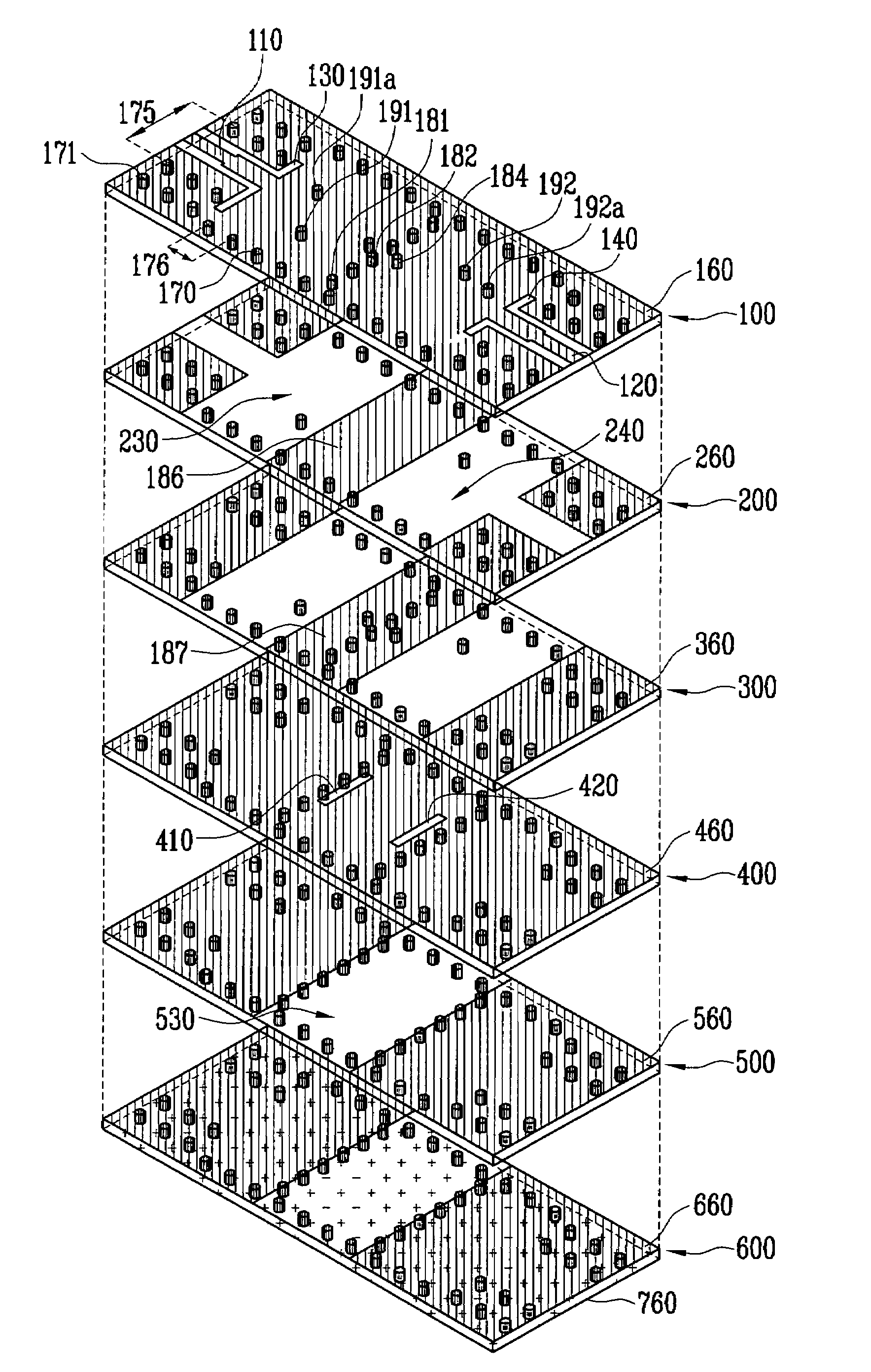
[0045]FIG. 3 is a perspective view illustrating a construction of a dielectric waveguide filter with cross-coupling according to the present invention.

[0046]Referring to FIG. 3, the inventive dielectric waveguide filter includes a first ground plane 160 and a second ground plane 760 at its top and bottom and a dielectric substrate with a multi-layered structure between the two ground planes 160 and 760. The dielectric waveguide filter further includes an input port 110 and an output port 120 (hereinafter, referred to as “input / output ports”) for connection with external systems and other devices; converters 130 and 140 for signal transition from a Transverse ElectroMagnetic (TEM) mode to a transverse electric (TE)10 mode; dielectric waveguide resonators 230, 240, and 530 providing a desired characteristic of the filter; vias 170 for forming each of dielectric waveguide resonators 230, 240, and 530; vias 171 for removing an unwanted waveguide mode; vias 181 and 182 for cross-coupling...

second embodiment

[0076]FIG. 7 illustrates the construction of a dielectric waveguide filter with cross-coupling according to the present invention.

[0077]Referring to FIG. 7, the inventive dielectric waveguide filter includes a first ground plane 160 and a second ground plane 760 at its top and bottom, and a dielectric substrate with a multi-layered structure between the two ground planes 160 and 760. The dielectric waveguide filter further includes an input port 110 and an output port 120 for connecting with external systems and other devices; converters 130 and 140 for transiting a signal from a transverse electromagnetic (TEM) mode to a transverse electric (TE)10 mode; dielectric waveguide resonators 230, 240, and 530 providing a desired characteristic of the filter; vias 170 for forming each of dielectric waveguide resonators 230, 240, and 530; vias 171 for removing an unwanted waveguide mode; vias 181, 182, and 184 for cross-coupling between the dielectric waveguide resonators 230 and 240 dispos...


PUM


Abstract

Provided is a dielectric waveguide filter. The filter includes: a multi-layered structure of dielectric substrates having first and second ground planes at its top and bottom; first, second, and third waveguide resonators disposed at multiple layers within the multi-layered structure; converters for signal transition between input / output ports and the first and third waveguide resonators; first vias for forming the first, second, and third waveguide resonators; and second vias disposed at a boundary surface of the first waveguide resonator and the third waveguide resonator.

Description

CROSS-REFERENCE TO RELATED APPLICATION[0001]This application claims priority to and the benefit of Korean Patent Application No. 2005-113486, filed Nov. 25, 2005, the disclosure of which is incorporated herein by reference in its entirety.BACKGROUND[0002]1. Field of the Invention[0003]The present invention relates to a dielectric waveguide filter with cross-coupling and a multi-layered resonator structure within multiple layers using a via and a pattern, and more particularly, to a dielectric waveguide filter used in a millimeterwave radio frequency (RF) front-end module of a 60 GHz pico cell communication system.[0004]2. Discussion of Related Art[0005]Wireless communication systems are expected to develop from a second generation wireless communication system for voice and character transmission to a third generation wireless communication system of an International mobile telecommunication-2000 (IMT-2000) for image information transmission and to a fourth generation wireless commu...

Claims


Application Information

Patent Timeline
Patent Type & Authority Patents(United States)
IPC IPC(8): H01P1/208
CPCH01P1/2088H01P1/207
Inventor JUN, DONG SUKCHO, KYOUNG IKLEE, HONG YEOLKIM, DONG YOUNGLEE, SANG SEOK
Owner ELECTRONICS & TELECOMM RES INST
Why Eureka
Try Eureka