Double trench for isolation of semiconductor devices

a technology of semiconductor devices and trenches, applied in the direction of semiconductor devices, basic electric elements, electrical equipment, etc., can solve the problems of symmetry breakage, termination and isolation of such structures, etc., and achieve the effect of improving performance and improving performan

Inactive Publication Date: 2010-02-23
AMI SEMICON BELGIUM
View PDF15 Cites 8 Cited by
  • Summary
  • Abstract
  • Description
  • Claims
  • Application Information

AI Technical Summary

Benefits of technology

[0010]This can help reduce the area needed for the electrical isolation between the active device and the other devices. Owing to the insulator in the first trench, there is no more depletion in the region next to the deep trench (because there is no junction termination). Thus, the isolation distance between the deep trench isolation and the first cell can be reduced down to e.g. 3 μm. Without this double trench approach, the isolation distance is determined by the required blocking capability, and is typically around 15 μm for 100V, and larger for higher voltages. Such reduction in area is commercially valuable and can enable greater integration or more cells in a multi cell power device, and so improve important performance parameters such as Ron.
[0017]Another such additional feature is the first trench having a conductive element within the first insulator. This can enable the trench to be used as a part of the device or to be biased to improve performance.
[0018]Another such additional feature is the second trench having a conductive element within the second insulator. Again this can enable the trench to be used as a part of the device or to be biased to improve performance.
[0028]The above double trench approach can provide junction termination of a super-MOS, for example as well as isolation of the complete super-MOS device from other devices on the same chip. The isolation distance can be substantially reduced compared to single trench isolation approaches. This can be achieved by a process using only two extra masks. Techniques that can contribute to smaller feature sizes can be valuable to semiconductor manufacturers in general and to those who integrate power devices in particular. In some such cases, reduction of the feature sizes can allow the integration of greater numbers of transistor cells per unit area. This can lead to lower ON resistance for a power transistor that has many unit cells acting in parallel.

Problems solved by technology

An important problem is the termination and isolation of such structures, when integrating such devices in a smart power platform with other devices.
At the periphery of the device, however, the symmetry is broken.

Method used


Image

  • Double trench for isolation of semiconductor devices
  • Double trench for isolation of semiconductor devices
  • Double trench for isolation of semiconductor devices

Examples


first embodiment

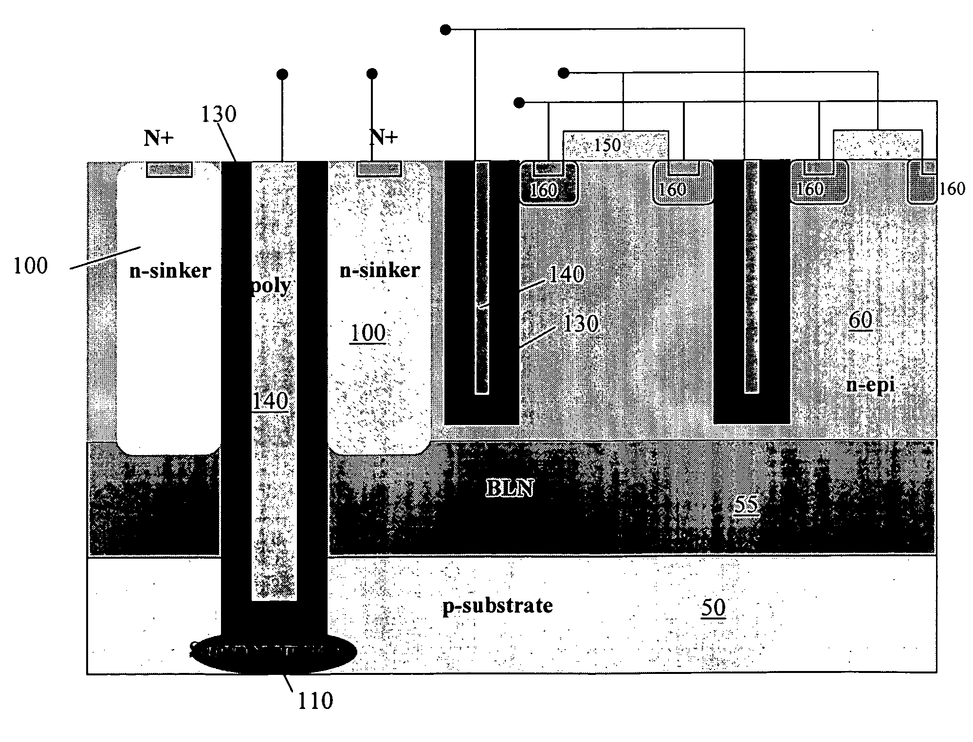
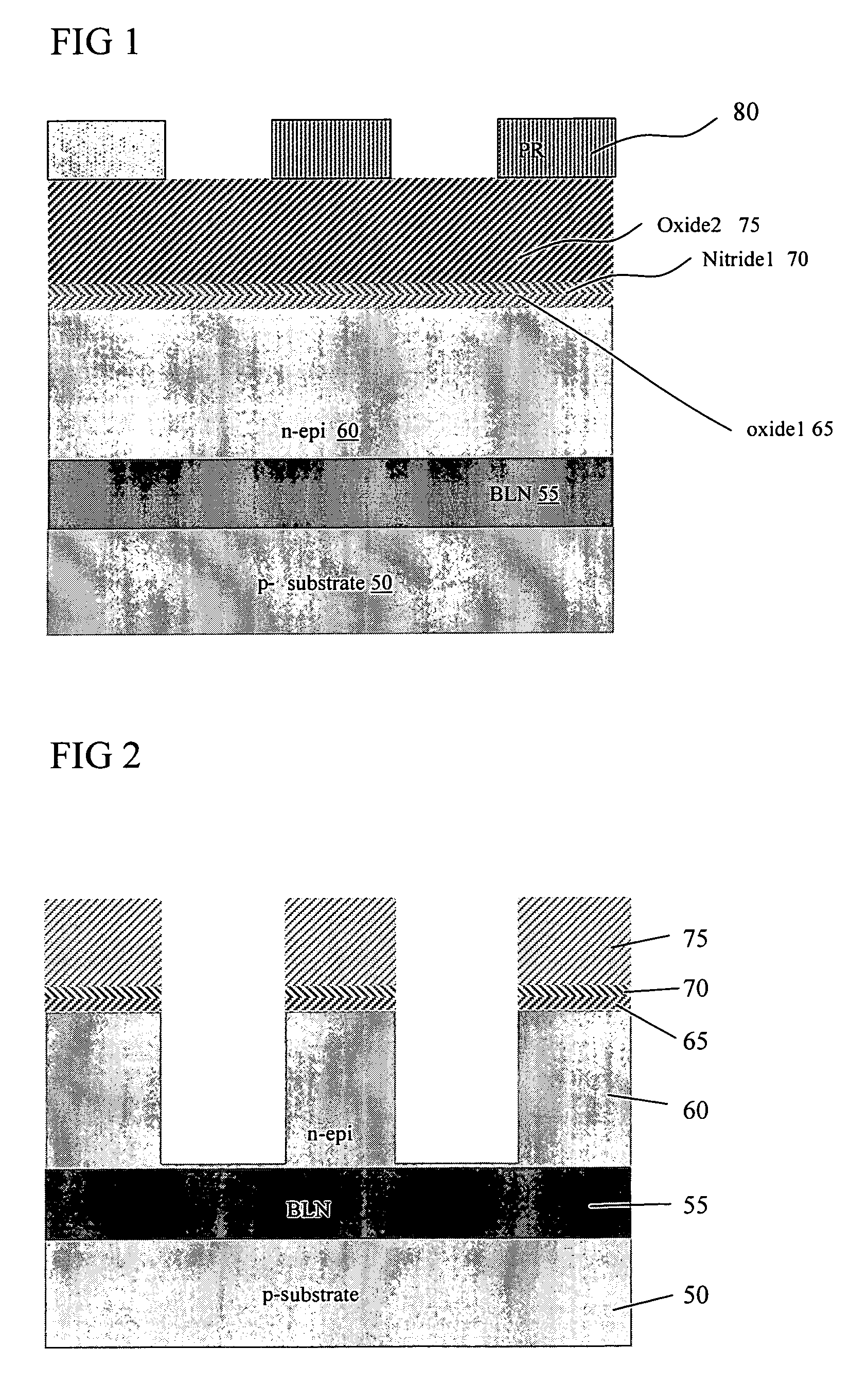
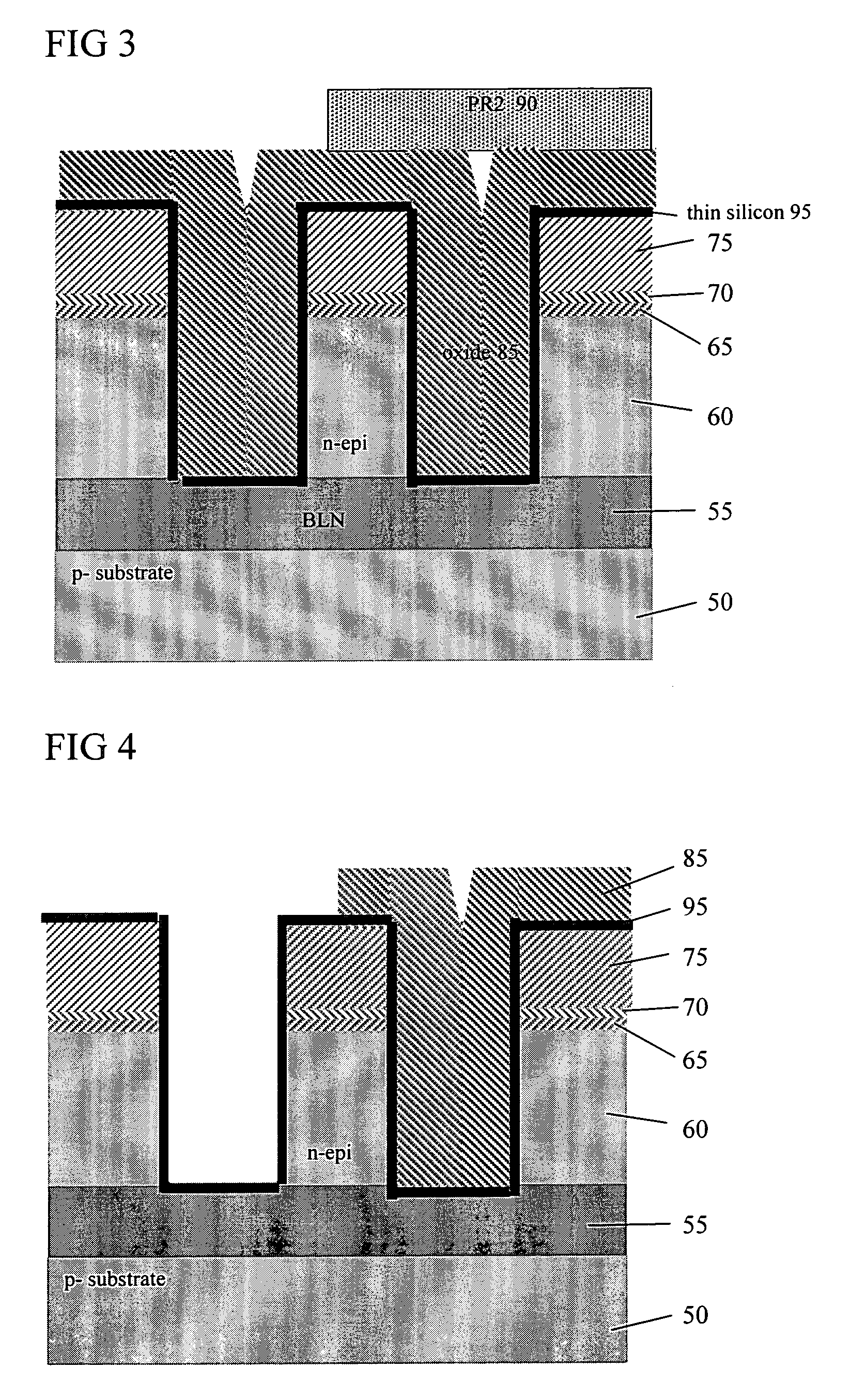
[0047](a) As shown in FIG. 1, on top of a lowly doped substrate of a first conductivity type, e.g. a p-substrate (˜1015-1016 atoms / cm3) 50 for example of silicon, and a highly doped buried layer of a second conductivity type, e.g. a highly doped buried n-type buried layer (˜1018-1019 atoms / cm3) 55, a moderately doped epitaxial layer of the second conductivity type, e.g. a moderately doped n-epi (˜1015-1016 atoms / cm3) layer 60 is grown. The concentration and thickness of the n-epi layer 60 is preferably tuned for optimal performance of the device, and is as such dependent on the targeted breakdown voltage Vbd. The thickness will be in the order of 3-10 μm for the voltage range of interest (50-200V). A thin insulating layer such as an oxide layer 65 (oxide1), having a thickness of about 15-40 nm, is grown on top of the n-epi layer 60. A thin insulating layer such as a thin nitride layer 70 (nitride1) having a thickness, for example of 20-50 nm, is subsequently deposited. Then, a thick...


PUM


Abstract

A semiconductor device has a substrate (50), a buried layer (55), an active area extending from a surface contact to the buried layer, an insulator (130) in a first trench extending towards the buried layer, to isolate the active area, and a second insulator (130) in a second deep trench and extending through the buried layer to isolate the buried layer and the active area from other parts of the substrate. This double trench can help reduce the area needed for the electrical isolation between the active device and the other devices. Such reduction in area can enable greater integration or more cells in a multi cell super-MOS device, and so improve performance parameters such as Ron. The double trench can be manufactured using a first mask to etch both trenches at the same time, and subsequently using a second mask to etch the second deep trench deeper.

Description

FIELD OF THE INVENTION[0001]This invention relates to semiconductor devices and methods of manufacturing such devices.DESCRIPTION OF THE RELATED ART[0002]The concept of super-MOS devices is used to drastically reduce the specific on resistance Ron for a given reverse breakdown voltage Vbd. Both vertical as well as lateral implementations are known. An important problem is the termination and isolation of such structures, when integrating such devices in a smart power platform with other devices. A super-MOS device contains an array or a matrix of unit cells. Hence, a unit cell in the center of the device sees a symmetric configuration: to the left and to the right of the unit cell the geometrical symmetry is conserved. At the periphery of the device, however, the symmetry is broken. As the operation of the transistor is based on the full depletion of the n-epi in between two cells, special precautions have to be taken to guarantee the reverse voltage capability at the periphery beca...

Claims


Application Information

Patent Timeline
Patent Type & Authority Patents(United States)
IPC IPC(8): H01L21/331H01L21/308H01L21/762
CPCH01L21/3081H01L21/3083H01L21/76205H01L21/76229H01L21/763
Inventor MOENS, PETERTACK, MARNIXBOONEN, SYLVIECOLSON, PAUL
Owner AMI SEMICON BELGIUM
Why Eureka
Try Eureka