Board-to-board connector

a technology of connectors and boards, applied in the direction of dielectric characteristics, coupling device connections, printed element electric connection formation, etc., can solve the problems of reduced binding strength between the contact and the post due to engagement, difficult bending of the contact, and difficulty in ensuring sufficient contact area, etc., to achieve the effect of convenient processing

Inactive Publication Date: 2010-03-09
MATSUSHITA ELECTRIC WORKS LTD
View PDF15 Cites 15 Cited by
  • Summary
  • Abstract
  • Description
  • Claims
  • Application Information

AI Technical Summary

Benefits of technology

[0007]To solve the above-mentioned problems, an object of the present invention is to provide a board-to-board connector which can perform simultaneous electrical and mechanical connection and achieve reduction in thickness as compared to conventional board-to-board connectors by eliminating connection between three-dimensional and complicated metal springs.
[0009]Since electrical and mechanical connection between the circuit boards can be performed in a two-dimensional way by using two components of the bump and the elastic body, it is unnecessary to use a three dimensional spring which requires space, achieving lower height and higher density. Furthermore, since electrical connection is performed by inserting the insertion hole of the elastic body and bringing the bump and the elastic body into contact with each other, an elastic effect is applied to the contact portion at attachment / detachment of the bump to / from the elastic body. Thus, when the bump is inserted, the umbrella section of the bump is caught in and engaged with the insertion hole of the elastic body, the bump can be prevented from slipping off the elastic body. Moreover, since this insertion hole is electrically connected to the conductive pattern, even when the bump is caught in any position in the insertion hole, electrical connection between the insertion hole and the bump can be maintained.
[0010]According to the present invention, in the improved board-to-board connector, the elastic body is formed of a substrate with circuit and a conductive rubber filled into a groove and a through hole which are formed on the substrate with circuit to be integrally molded, and the conductive pattern is formed of a circuit of the substrate and the conductive rubber. Thus, since the conductive rubber becomes the conductive pattern and is electrically connected to the bump, there is no need to form a circuit pattern for contact against the bump by means of plating or the like, resulting in simple manufacturing processes. Moreover, since the through hole is made of the conductive rubber, compared with the case the bump is inserted into the through hole made of a copper foil, there is less possibility that the conductive pattern is chipped or peeled off due to insertion of the umbrella section of the bump into the through hole. Furthermore, the through hole can be configured using the conductive rubber only at the area of the substrate with circuit into which the bump is inserted. Thus, since the whole of the substrate with circuit 51a need not be elastic, an inexpensive circuit board can be used, resulting in lower costs.
[0011]According to the present invention, in the improved board-to-board connector, the elastic body is formed of a substrate with circuit and a conductive rubber integrally molded on the substrate with circuit and in a through hole formed on the substrate, and the conductive pattern is formed of a circuit of the substrate and the conductive rubber. Thus, since the conductive pattern is integrally formed on the substrate and in the through hole without forming a groove on the circuit board, manufacturing processes become simple, leading to reduction in manufacturing costs. Further, groove processing of further decreasing the intensity of the thin substrate having low intensity is not carried out, the intensity of the connector can be prevented from lowering.
[0013]According to the present invention, in the improved board-to-board connector, the conductive rubber sheet has a copper foil and the copper foil is joined to a joining pattern provided on the insulative substrate with circuit. Thus, since the conductive rubber sheet has the copper foil, the copper foil can be joined to the insulative substrate with circuit. By removing an unnecessary portion from the rubber sheet with copper foil by mechanical processing with the copper foil being stuck, joining the molded rubber sheet with copper foil to the insulative substrate with circuit through the copper foil and then, mechanically removing the unnecessary portion again, the conductive rubber sheet can be easily processed and formed on the substrate.

Problems solved by technology

However, from the perspective of further reduction in size and thickness, since the connector disclosed in the above-mentioned Patent document 1 has the structure that the inner side surface of the dead end portion of the contact is brought into contact with the outer side surface of the post for electrical connection, when one attempts to make the structure thinner, bending of the contact becomes difficult.
In addition, when the contact portion is shortened, sufficient contact area is hard to be ensured and binding strength between the contact and the post due to engagement is decreased.
Thus, disadvantageously, the engagement is easy to be released.
However, since the housing, into where the contact and the post are press-fit, is made of synthetic resin, there is a limitation in reducing the size of the housing due to workability and strength, making it more difficult to reduce the pitch.
Furthermore, since minimum thickness of the housing is needed to stand press-fitting of the contact and the post, it is difficult to reduce the height of the connector.
Thus, obviously, there is a limitation in lower height (thinner size) and higher density.

Method used


Image

  • Board-to-board connector
  • Board-to-board connector
  • Board-to-board connector

Examples


first embodiment

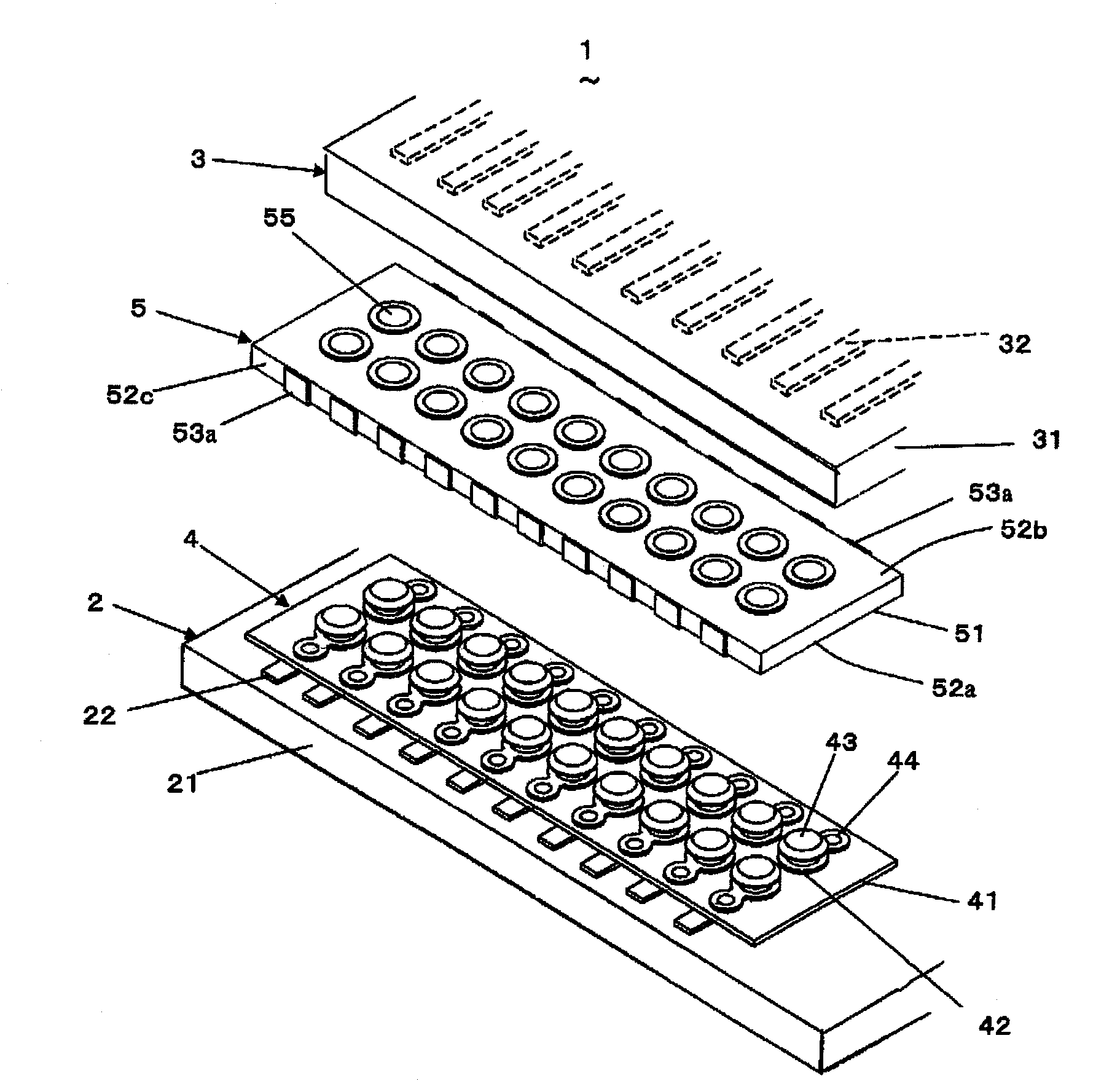
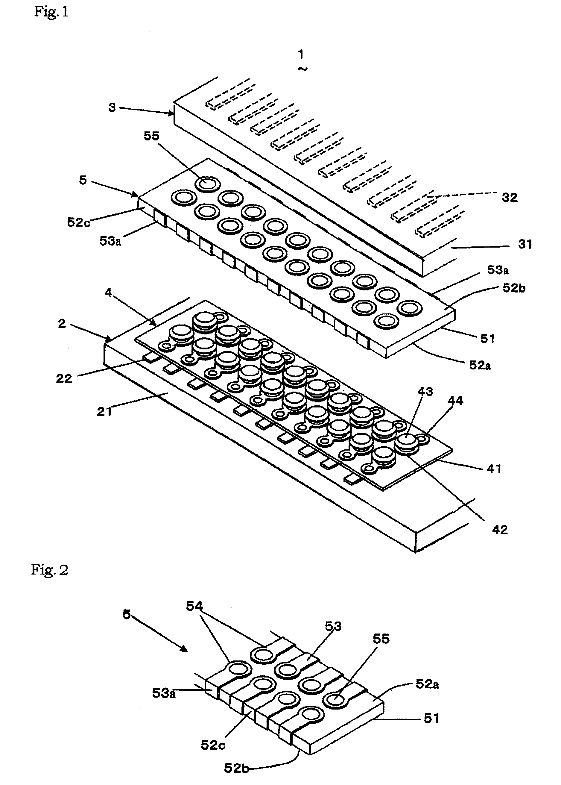
[0057]Hereinafter, a board-to-board connector in accordance with First embodiment of the present invention will be described with reference to FIG. 1 to FIG. 5. The board-to-board connector 1 in this embodiment has a first connector 4 and a second connector 5 for board-to-board connection, which are connected to circuit boards 2 and 3, respectively. The first connector 4 and the second connector 5 are electrically connected to a circuit pattern 22 formed on an insulative substrate 21 of the circuit board 2 and a circuit pattern 32 formed on an insulative substrate 31 of the circuit board 3, respectively. The board-to-board connector 1 connects the circuit boards 2, 3 by connecting the first connector 4 to the second connector 5.

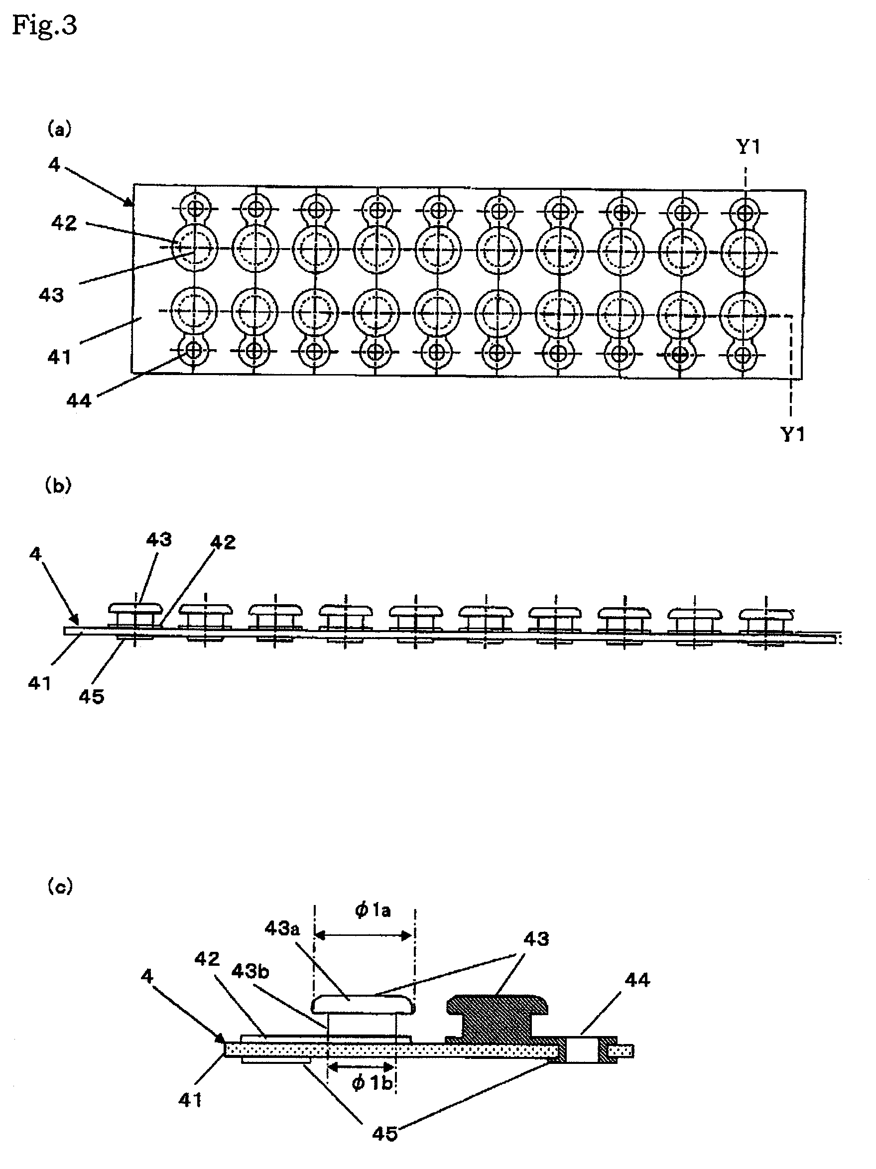
[0058]As shown in FIG. 1, the first connector 4 has a substrate 41 made of an insulative member and a conductive pattern 42 provided on the surface of the substrate 41 (the upper surface in FIG. 1). On the conductive pattern 42 are provided a conductive bump ...

second embodiment

[0080]The connector 4 is connected to the connector 5 by inserting the bump 43 into the elastic conductive section 62 of the connector 5. This connection is the same as the connection in Second embodiment except that the elastic conductive section 62 protrudes from the surface of the substrate 51a on the connection plane of the connector 5 by the height d2 of the gate 64, detailed description thereof is omitted.

[0081]As described above, according to this embodiment, since the conductive pattern is integrally formed on the substrate 51 and in the through hole 55 without forming a groove on the circuit board, manufacturing processes become simple, leading to reduction in manufacturing costs. Further, groove processing of further decreasing the intensity of the thin substrate having low intensity is not carried out, the intensity of the connector can be prevented from lowering. Furthermore, since the conductive rubber 6 protrudes from the surface of the substrate 51 by the height of th...

third embodiment

[0083]In the second connector 5, the elastic substrate 51, as shown in FIG. 16, FIG. 17, comprises the insulative substrate 51a having a circuit pattern (conductive pattern) connected to each surface thereof through the through hole 55 and the conductive rubber sheet 6a obtained by making the conductive rubber 6 in the shape of a sheet. A copper foil 7 is stuck on the surface of the conductive rubber sheet 6a and a copper foil pattern 71 of the copper foil 7 is integrated with the conductive pattern 61 of the conductive rubber sheet 6a. The elastic conductive section 62 having the through hole 63 into which the bump 43 of the first connector 4 is inserted is formed on the conductive rubber sheet 6a. The through hole 73 corresponding to the through hole 63 of the conductive pattern 61 is provided on the copper foil pattern 71. A land pattern 72 joined to the circuit conductive pattern 53 of the substrate 51a is provided on the copper foil pattern 71 surrounding the through hole 73. T...


PUM


Abstract

A thin board-to-board connector with high density in which there is no connection between three-dimensional complex metal springs. The board-to-board connector includes a connector having a bump for electrical connection having an umbrella shape on a board and connected to a circuit board and a connector having an elastic electrically conductive section having a through hole made in a conductive pattern on an elastic insulating board and connected to a circuit board electrically connected to the elastic conductive section. When a bump is inserted into the through hole, the elastic conductive section is electrically connected to the bump, and the side surface of the through hole is pressed against to the bump and elastically deformed and dented. Consequently, the bump is press-fit into the through hole. With this, the bump can be inserted into the elastic conductive section and engaged with it, and thereby electrical and mechanical connection between circuit boards can be simultaneously achieved in a two-dimensional manner, realizing a low-height connector.

Description

TECHNICAL FIELD[0001]The present invention relates to a board-to-board connector used in a compact and slim electronic devices.BACKGROUND ART[0002]The board-to-board connector for connecting electronic circuits on two opposed printed circuit boards to each other is used as a connector used in electronic devices such as mobile phones and digital cameras which have been reduced in size and weight. In the board-to-board connector, one of the connected printed circuit board has a socket and the other of the connected printed circuit board has a header. By connecting the socket to the header, electronic circuits formed on both the printed circuit boards are connected to each other.[0003]In this type of conventional board-to-board connector, as disclosed in, for example, Unexamined Patent Publication No. 2004-055464, a contact obtained by bending a strip conductor in the shape of a dead end is provided at the socket as one connector, and a post having a conductor protruding from the heade...

Claims


Application Information

Patent Timeline
Patent Type & Authority Patents(United States)
IPC IPC(8): H01R12/00H01R12/79
CPCH01R12/57H01R12/58H05K3/368H01R12/523H05K3/326H05K3/4007H05K3/42H05K2201/0133H05K2201/0367H05K2201/10378
Inventor TANAKA, HIROHISAHASHIMOTO, SHUNSUKE
Owner MATSUSHITA ELECTRIC WORKS LTD
Why Eureka
Try Eureka