Circuit board structure having capacitor array and embedded electronic component and method for fabricating the same

a capacitor array and circuit board technology, applied in the direction of printed capacitor incorporation, association of printed circuit non-printed electric components, electrical apparatus construction details, etc., can solve the problems of reduced circuit volume, increased noise accompanying with it, and difficulty in reducing the overall size of the semiconductor package, so as to simplify the fabrication procedure

Active Publication Date: 2010-03-09
PHOENIX PRECISION TECH CORP
View PDF1 Cites 13 Cited by
  • Summary
  • Abstract
  • Description
  • Claims
  • Application Information

AI Technical Summary

Benefits of technology

[0011]Still another objective of the invention is to provide a circuit board having a capacitor array and embedded electronic components and a method of fabricating the same, in which the capacitor components are formed in a simple fabricating method, so that the prior art problems of complexity in disposing circuit due to the electronic elements mounted on the surface and insufficient disposing space are solved.
[0012]A further objective of the invention is to provide a circuit board having a capacitor array and embedded electronic components and a method of fabricating the same, in which the capacitor components are formed in a simple fabricating method so as to prevent complexity in fabrication due to the process of embedding passive components between circuit board layers.
[0020]As such, the circuit board having a capacitor array and embedded electronic components and the method of making the same proposed by the invention permits the development of low-profile circuit board, as well as eliminating the requirement of surface mounting technology (SMT)) for forming passive components on the surface of the circuit board, thereby solving the prior art problem of limited space for disposing circuit on the circuit board, as well as simplifying fabricating procedure by eliminating the complicated process of embedding passive components in a multi-layered circuit board. Moreover, peeling issue resulted from the large difference of coefficient of thermal expansion (CTE) between the dielectric layer and embedded passive components in the prior art can be solved.

Problems solved by technology

In the condition where the number of leads and circuit complexity are increased but the circuit volume is decreased, the noise accompanying with it is also increases.
However this method requires a relative larger surface area of the circuit board, thereby making it difficult to reduce the overall size of the semiconductor package.
Moreover these passive components are often mounted into different regions of the circuit board, thereby increasing the difficulty of disposing circuit and the complexity of fabricating process.
This type of arrangement although increases the circuit disposing area but the effectiveness of eliminating noise and stabilizing circuit is decreased accordingly.
Moreover, as the semiconductor device is developed toward high functionality, the number of passive components 12 in the package is increased accordingly, therefore using conventional method, the volume of semiconductor package would be increased so as to accommodate semiconductor chips 11 and large number of passive components 12, thereby making it not possible to meet the requirement of low-profile package.
Although the technology of forming embedded film-like passive components between each layers of the multi-layered circuit board can solve the problem of limitation of available circuit disposing area in the prior art, the fabricating process of forming embedded passive components between each layers of the multi-layered circuit board is complex and moreover because of the large difference of coefficient of thermal expansion (CTE) between the dielectric layer and embedded passive components, a peeling issue is often involved in the fabricating process.

Method used


Image

  • Circuit board structure having capacitor array and embedded electronic component and method for fabricating the same
  • Circuit board structure having capacitor array and embedded electronic component and method for fabricating the same
  • Circuit board structure having capacitor array and embedded electronic component and method for fabricating the same

Examples


Embodiment Construction

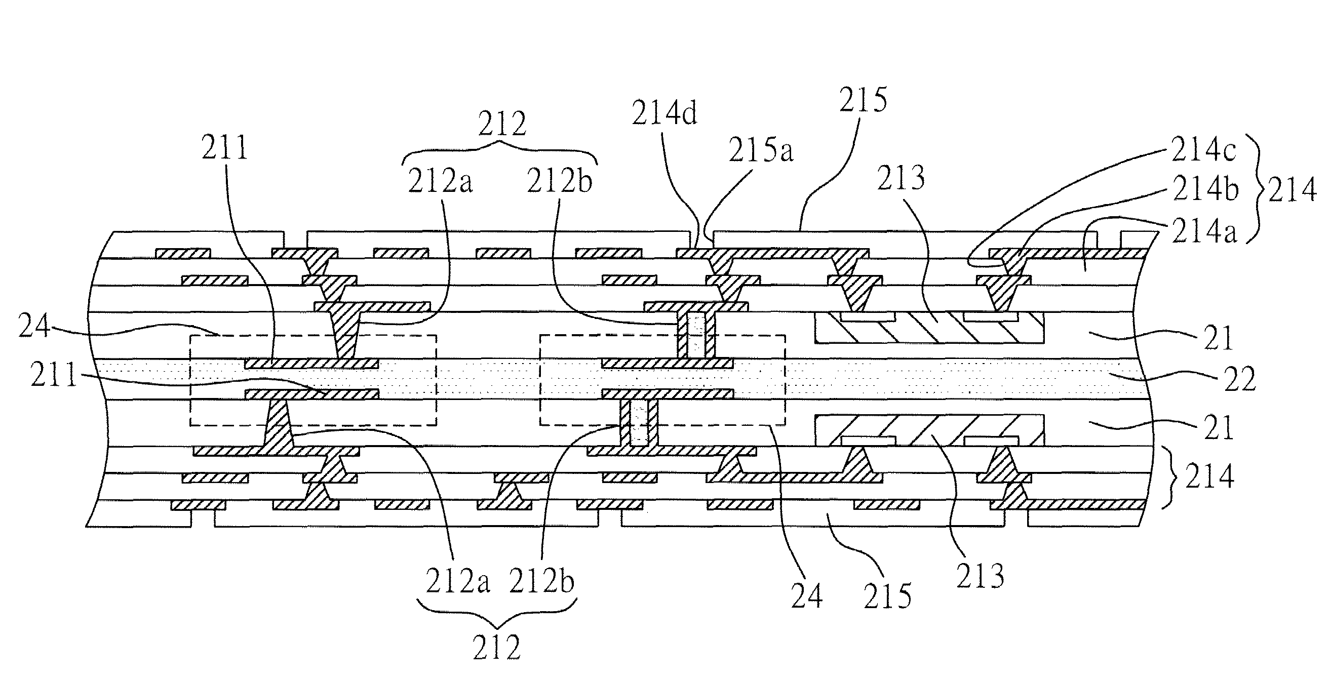
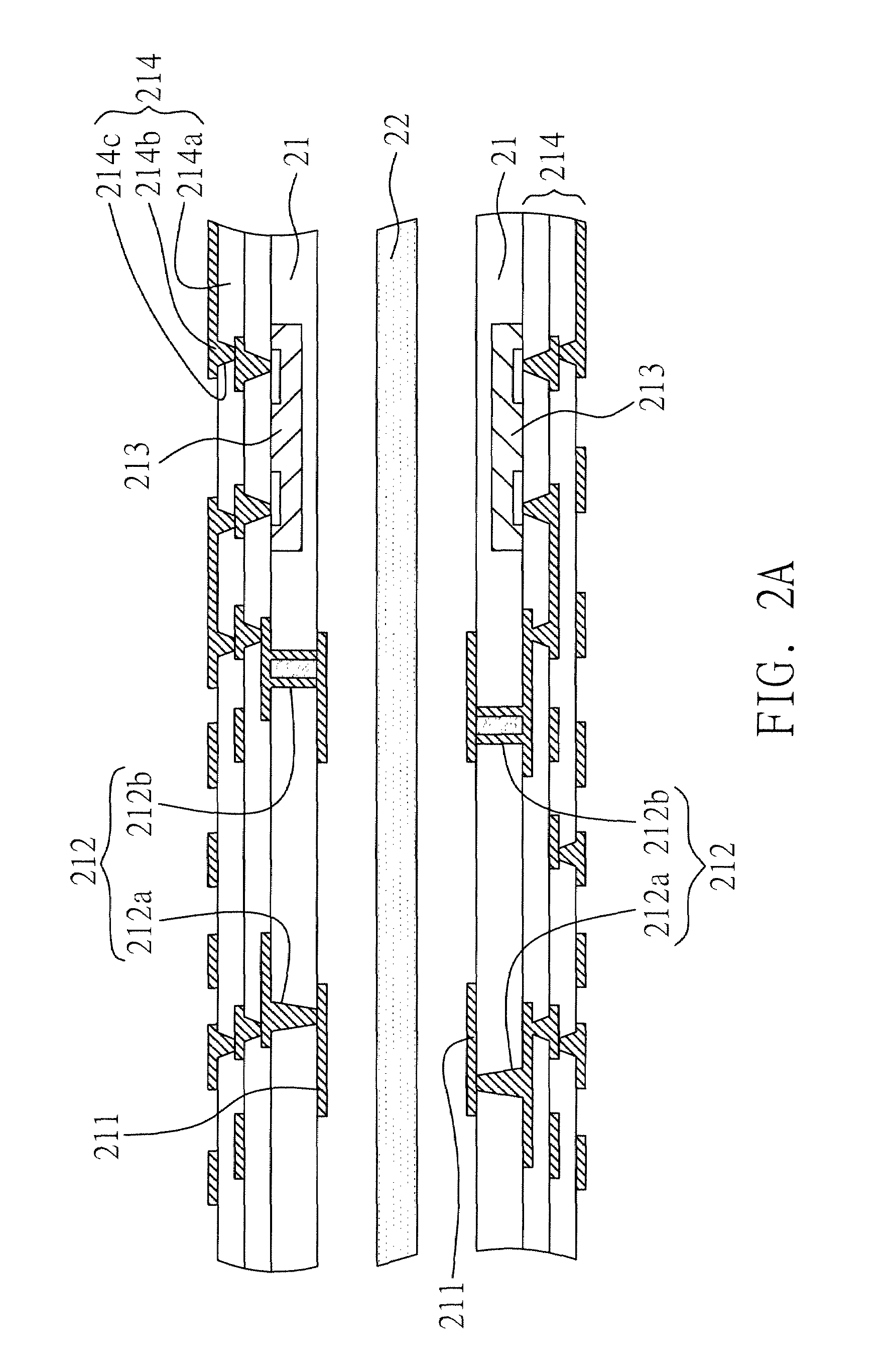
[0026]The present invention is described in the following with specific embodiments, so that one skilled in the pertinent art can easily understand other advantages and effects of the present invention from the disclosure of the invention. The present invention may also be implemented and applied according to other embodiments, and the details may be modified based on different views and applications without departing from the spirit of the invention. In addition, the drawing and the components shown herein are not to scale and are made in simplicity with provision of only associated components related to the invention; in practical usage, the component should e more complexly structured and the number, size, shape and arrangement of each component can be varied accordingly.

[0027]Referring to FIGS. 2A and 2B, a schematic cross-sectional view showing a method of fabricating a circuit board having a capacitor array and embedded electronic components of the present invention are provid...


PUM


Abstract

A circuit board structure having a capacitor array and an embedded electronic component and a method for fabricating the same are proposed. Two carrier boards and a high dielectric constant material layer are provided, wherein the carrier boards have electronic components embedded therein and one surface of each carrier board has a plurality of electrode plates. The two carrier boards are laminated with the dielectric constant material layer interposed between them. The electrode plates on the surfaces of the carrier boards are opposite to each other across the high dielectric constant material layer to constitute a capacitor array. Therefore, the capacitor assembly for design of electronic devices is provided.

Description

FIELD OF THE INVENTION[0001]The present invention relates to circuit boards having capacitor arrays and embedded electronic components, and methods of making the same, and more particularly to a circuit board having a capacitor array formed by laminating carrier boards having embedded electronic components and electrode plates having capacitors on one surface of the carrier board and a method of making the same.BACKGROUND OF THE INVENTION[0002]Due to the rapid growth in the electronic industry, electronic devices have gradually been developed towards the direction of multi-function, high speed and low-profile, and as a result reducing surface area of circuit board and miniaturization of the package are the two primary targets in the electronic industry. In the demand of high integration and miniaturization of semiconductor packages, many have adopted a multi-chip module (MCM) with multi-layer board using the technology of interlayer connection so as to increase the usable surface ar...

Claims


Application Information

Patent Timeline
Patent Type & Authority Patents(United States)
IPC IPC(8): H05K1/16
CPCH05K1/162H05K1/185H05K3/4602H05K3/4626H05K2201/0209H05K2201/09536H05K2201/09672H05K2203/061H01L24/19H01L2224/04105H01L2924/14H01L2924/00
Inventor CHANG, CHIA-WEILIEN, CHUNG-CHENG
Owner PHOENIX PRECISION TECH CORP
Why Eureka
Try Eureka