

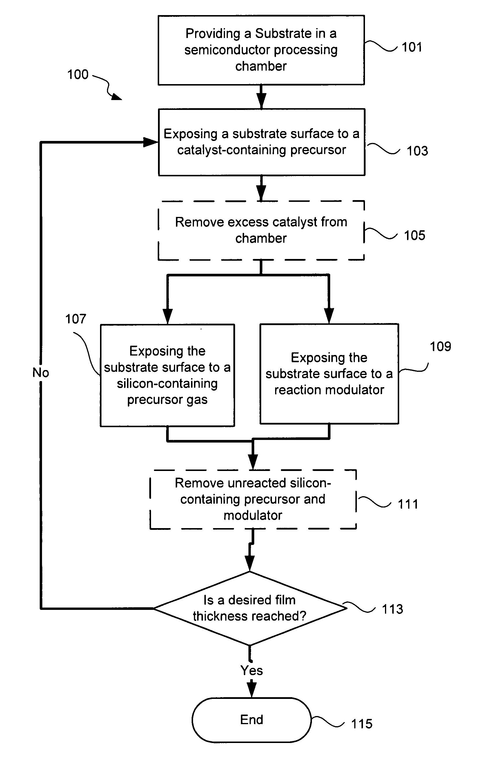
Method of forming low-temperature conformal dielectric films
a dielectric film, low-temperature technology, applied in the direction of chemical vapor deposition coating, semiconductor/solid-state device details, coatings, etc., can solve the problem of increasing the depth to width of features, the deposition rate is very low, and the traditional cvd techniques cannot provide void-free gap-filling in high aspect ratio features. to achieve the effect of acceleration or quenching the reaction
- Summary
- Abstract
- Description
- Claims
- Application Information
AI Technical Summary
Benefits of technology
Problems solved by technology
Method used
Image

Examples
example
[0050]The following example provides details relating to performance advantages of the present invention. It should be understood the following is representative only, and that the invention is not limited by the detail set forth in this example.
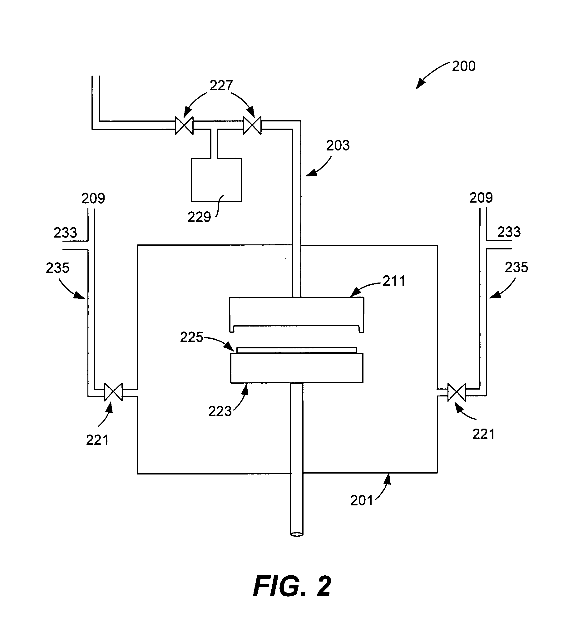
[0051]The method of the invention was implemented by a PDL process using trimethylaluminum (Al(CH3)3) (TMA) as a metal-containing catalyst and tris(tert-pentoxy)silanol((C5H11O)3SiOH; TPOSL; MW=306) as the silicon-containing precursor. In one case, the TPOSL precursor included one percent (1%) reaction accelerator, which is believed to be a chloro alkoxy silane, and in another case, the TPOSL precursor did not include a reaction accelerator.
[0052]FIG. 4 is a plot of the chamber pressure over time for both cases. The chamber pressure for deposition including a reaction accelerator is shown as line 401. The chamber pressure for deposition not including a reaction accelerator is shown as line 403. Referring to line 401 at the beginning of the f...
PUM
| Property | Measurement | Unit |
|---|---|---|
| depths | aaaaa | aaaaa |
| temperatures | aaaaa | aaaaa |
| temperatures | aaaaa | aaaaa |
Abstract
Description
Claims
Application Information