Multistep method of depositing metal seed layers

Active Publication Date: 2010-03-23
NOVELLUS SYSTEMS
View PDF153 Cites 45 Cited by
  • Summary
  • Abstract
  • Description
  • Claims
  • Application Information

AI Technical Summary

Benefits of technology

[0006]The present invention provides a method of depositing metal seed layers on a semiconductor substrate having recessed features. In this method, a first layer of metal is deposited onto the substrate to cover at least the bottom portions of the recessed features. The first layer of metal is subsequently redistributed to improve sidewall coverage of the recessed features. Next, a second layer of metal is deposited on at least the field region of the substrate and on the bottom portions of the recessed features. This sequence of operations can produce seed layers

Problems solved by technology

Further, improved seed layer coverage decreases undesirable impact of the terminal effect that is ofte

Method used


Image

  • Multistep method of depositing metal seed layers
  • Multistep method of depositing metal seed layers
  • Multistep method of depositing metal seed layers

Examples


examples

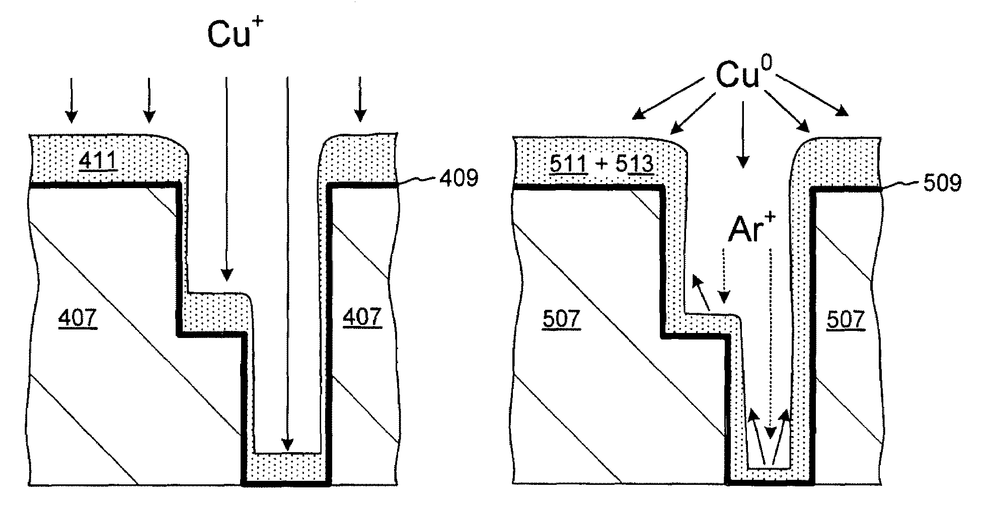
[0096]The methods of present invention have been evaluated experimentally. FIG. 7A presents an experimental plot that illustrates probability of device having a particular via chain resistance for devices fabricated using three different seed layer formation methods. Curve (a) illustrates the devices, fabricated using a deposition-resputter-deposition seed layer formation sequence provided by methods described herein. Curve (b) corresponds to devices fabricated using a deposition-resputter two-step seed layer formation method, and curve (c) corresponds to devices fabricated using a one-step deposition only method.

[0097]It can be seen that parametric performance of devices fabricated using deposition / resputter / deposition method, illustrated by curve (a), is superior to the performance of devices fabricated using other methods. Thus, only minor variation in via chain resistance is observed in the devices illustrated by curve (a). At the same time, the probability of device formation w...


PUM

PropertyMeasurementUnit
Fractionaaaaaaaaaa
Fractionaaaaaaaaaa
Fractionaaaaaaaaaa

Abstract

Metal seed layers are deposited on a semiconductor substrate having recessed features by a method that involves at least three operations. In this method, a first layer of metal is deposited onto the substrate to cover at least the bottom portions of the recessed features. The first layer of metal is subsequently redistributed to improve sidewall coverage of the recessed features. Next, a second layer of metal is deposited on at least the field region of the substrate and on the bottom portions of the recessed features. The method can be implemented using a PVD apparatus that allows deposition and resputtering operations. This sequence of operations can afford seed layers with improved step coverage. It also leads to decreased formation of voids in interconnects, and to improved resistance characteristics of formed IC devices.

Description

FIELD OF THE INVENTION[0001]The present invention pertains to methods of depositing layers of material on a partially fabricated integrated circuit. The methods are particularly useful for depositing metal seed layers, such as copper seed layers in Damascene processing.BACKGROUND OF THE INVENTION[0002]Damascene processing is a method for forming metal lines on integrated circuits. It involves formation of inlaid metal lines in trenches and vias formed in a dielectric layer (inter metal dielectric). Damascene processing is often a preferred method because it requires fewer processing steps than other methods and offers a higher yield. It is also particularly well-suited to metals such as copper that cannot be readily patterned by plasma etching.[0003]In a typical Damascene process flow, metal is deposited onto a patterned dielectric to fill the vias and trenches formed in the dielectric layer. The resulting metallization layer is typically formed either directly on a layer carrying a...

Claims


Application Information

Patent Timeline
IPC IPC(8): H01L23/535
CPCC23C14/046C23C14/5826C23C14/584H01L21/2855H01L21/76843H01L21/76862H01L21/76873H01L21/76865
Inventor ROZBICKI, ROBERTVAN SCHRAVENDIJK, BARTMOUNTSIER, TOMWU, WEN
Owner NOVELLUS SYSTEMS
Why Eureka
Try Eureka