Atomic layer profiling of diffusion barrier and metal seed layers

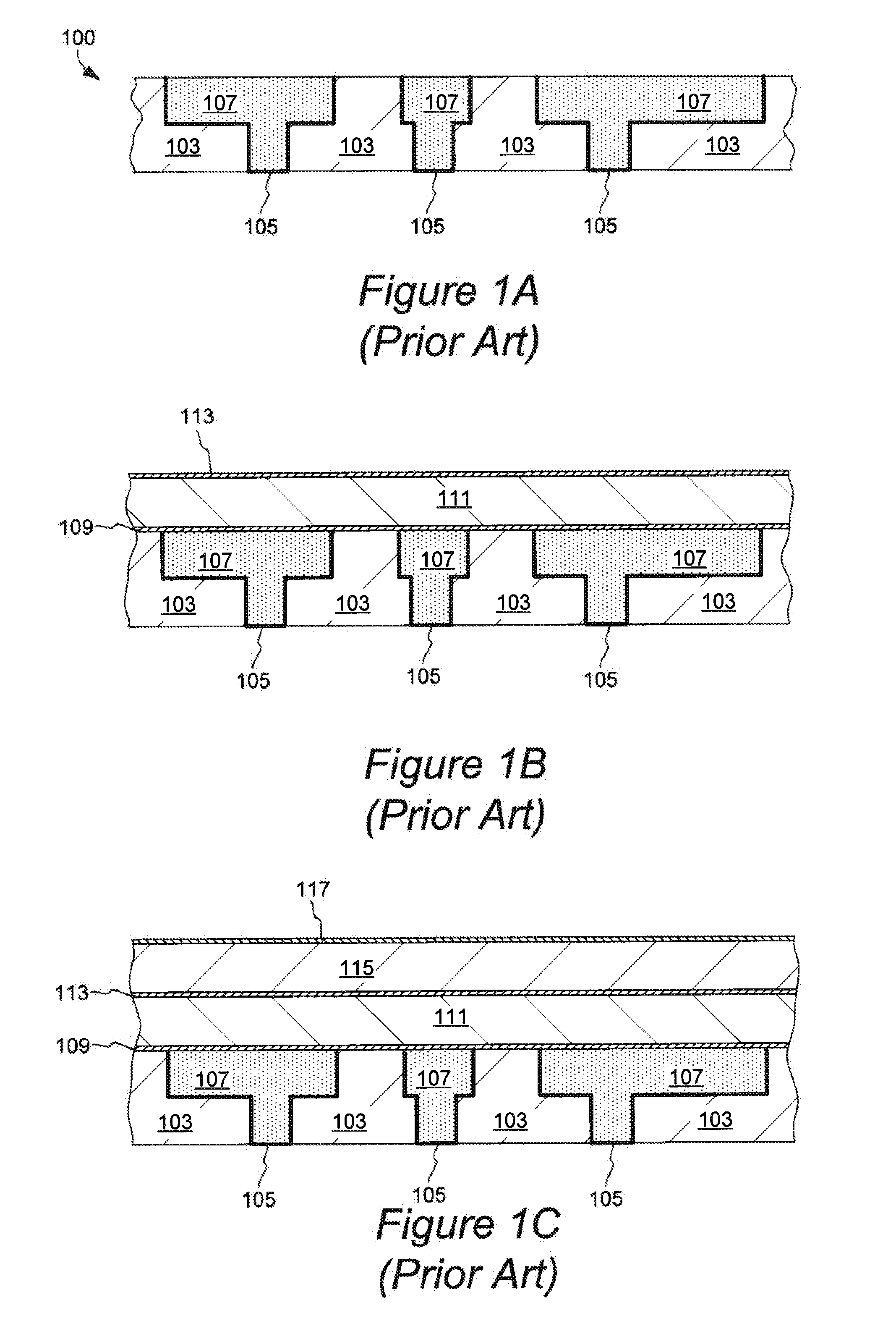
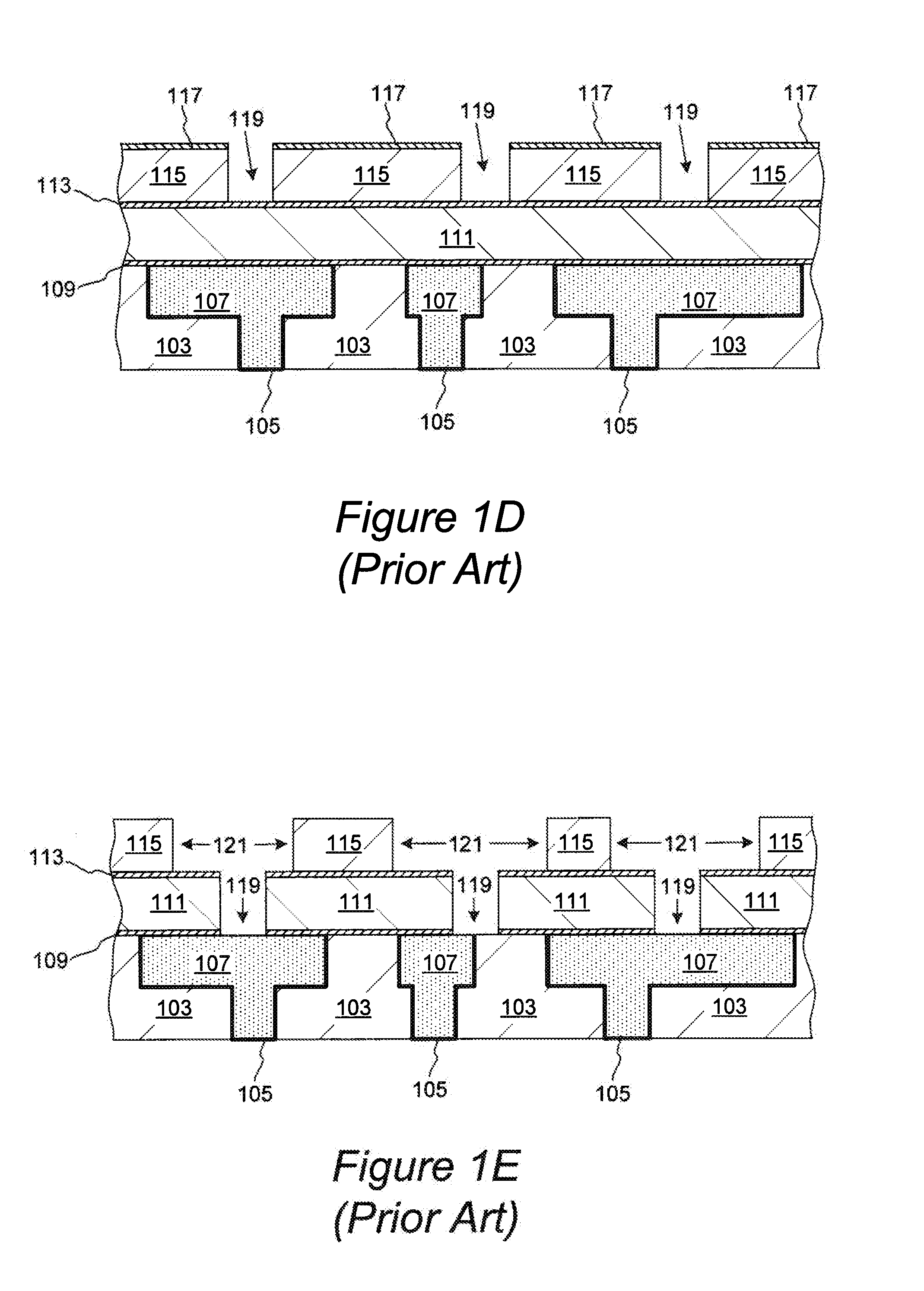
a diffusion barrier and layer profiling technology, applied in the direction of sputtering coating, vacuum evaporation coating, coating, etc., can solve the problems of easy damage to exposed dielectric materials, microtrenching damage, and more difficult to perform resputtering without exposing dielectric layers to plasma, so as to improve the shape of the feature bottom, improve the sidewall coverage of recessed features, and reduce overhang

Active Publication Date: 2010-11-30
NOVELLUS SYSTEMS
View PDF191 Cites 17 Cited by
  • Summary
  • Abstract
  • Description
  • Claims
  • Application Information

AI Technical Summary

Benefits of technology

[0017]In other embodiments, provided methods are applied to resputtering of copper seed layers. Resputtering of copper seed layers is often performed to improve sidewall coverage of recessed features and to reduce overhang at the recessed feature openings. Performing resputtering in a series of profiling cycles achieves improved shaping of the feature bottom, and improved overhang reshaping.
[0018]Further, resputtering in a series of profiling cycles achieves more rounded feature bottoms, leading to improved coverage in this region. In particular, material coverage in the bottom corners of recessed features can be significantly improved. For example, at least about 5 Å diffusion barrier or seed layer coverage can be obtained at the bottom corners of the recessed features with the use of provided methods.

Problems solved by technology

With an ongoing miniaturization of IC devices, especially with processing of devices at a 65 nm technology node and at more advanced nodes, it became more challenging to perform resputtering without exposing dielectric layers to plasma.
When resputtering is performed under conventional conditions, the exposed dielectric material can easily become damaged by high-energy ions that impinge upon it.
One type of such damage is microtrenching, which manifests itself in increased dielectric etching at particular locations within the recessed features of the wafer.
Microtrenching leads to decreased reliability of the formed IC devices due to reduced adhesion of the subsequently deposited layers.
Further, microtrenching contributes to an increase in line-to-line leakage due to a local increase in current densities in the microtrenches.

Method used


Image

  • Atomic layer profiling of diffusion barrier and metal seed layers
  • Atomic layer profiling of diffusion barrier and metal seed layers
  • Atomic layer profiling of diffusion barrier and metal seed layers

Examples


Embodiment Construction

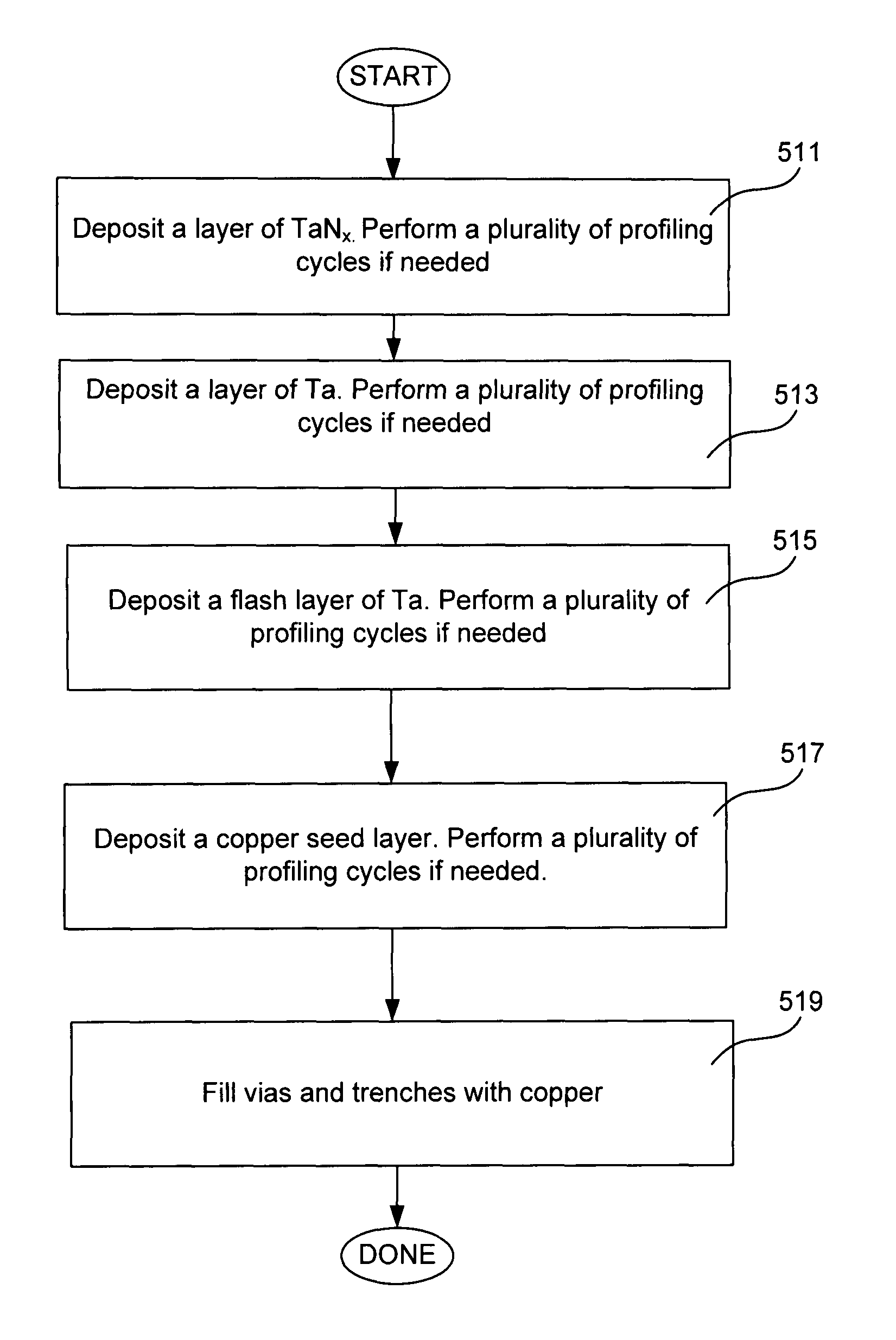
[0031]Plasma etch-back (resputtering) of metal-containing materials on a wafer is performed using a plurality of atomic layer profiling (ALP) cycles. Each cycle includes a net etch operation and a net deposition operation. Small amounts of material are etched and deposited in each operation, resulting in a net etch-back which could be performed incrementally, often with an atomic scale control. Several benefits can be achieved with the use of this method. First, it was discovered that plasma etching that employs alternating etching and depositing operations can be used to remove metal-containing materials from the wafer surface in the presence of an exposed dielectric without causing microtrenching in a dielectric. Further, it was noted that improved overhang clipping can be achieved with this method compared to a one-step resputtering. Also, profiling cycles described herein can be used to improve the shapes of recessed features, making them more rounded at the bottom. Provided met...


PUM

PropertyMeasurementUnit
widthsaaaaaaaaaa
widthsaaaaaaaaaa
RF poweraaaaaaaaaa

Abstract

Material is removed from a substrate surface (e.g., from a bottom portion of a recessed feature on a partially fabricated semiconductor substrate) by subjecting the surface to a plurality of profiling cycles, wherein each profiling cycle includes a net etching operation and a net depositing operation. An etching operation removes a greater amount of material than is being deposited by a depositing operation, thereby resulting in a net material etch-back per profiling cycle. About 2-10 profiling cycles are performed. The profiling cycles are used for removing metal-containing materials, such as diffusion barrier materials, copper line materials, and metal seed materials by PVD deposition and resputter. Profiling with a plurality of cycles removes metal-containing materials without causing microtrenching in an exposed dielectric. Further, overhang is reduced at the openings of the recessed features and sidewall material coverage is improved. Integrated circuit devices having higher reliability are fabricated.

Description

CROSS-REFERENCE TO RELATED APPLICATIONS[0001]This application is a continuation-in-part claiming priority under 35 USC 120 from U.S. patent application Ser. No. 11 / 588,586 filed Oct. 26, 2006 (now U.S. Pat. No. 7,781,327 issued Aug. 24, 2010), titled “Resputtering Process for Eliminating Dielectric Damage”, naming Kailasam et al. as inventors, which is a continuation-in-part of U.S. application Ser. No. 10 / 804,353 now U.S. Pat. No. 7,186,648 filed Mar. 18, 2004 (issued Mar. 6, 2007), titled “Barrier First Method For Single Damascene Trench Applications,” naming Rozbicki et al. as inventors which is a continuation-in-part of U.S. application Ser. No. 10 / 412,562 now U.S. Pat. No. 6,764,940 filed Apr. 11, 2003 (issued Jul. 20, 2004) titled “Method For Depositing A Diffusion Barriers For Copper Interconnect Applications,” naming Rozbicki and Danek as inventors. Each of these references is incorporated herein by reference in its entirety for all purposes.FIELD OF THE INVENTION[0002]The p...

Claims


Application Information

Patent Timeline
Patent Type & Authority Patents(United States)
IPC IPC(8): H01L21/4763
CPCC23C14/046C23C14/345H01L21/2855H01L21/76805H01L21/76843H01L21/76865
Inventor PRADHAN, ANSHU A.ROZBICKI, ROBERT
Owner NOVELLUS SYSTEMS
Why Eureka
Try Eureka