Method of forming a contact in a semiconductor device with formation of silicide prior to plasma treatment

a technology of silicide and contact, which is applied in the manufacturing of semiconductor/solid-state devices, basic electric elements, electric devices, etc., can solve the problems of short substrate, insufficient thickness of less desirable thick titanium nitride barrier metal layer in more highly integrated circuits

Inactive Publication Date: 2005-08-09
GLOBALFOUNDRIES INC
View PDF2 Cites 4 Cited by
  • Summary
  • Abstract
  • Description
  • Claims
  • Application Information

AI Technical Summary

Benefits of technology

[0008]There is a need for an improved method of forming contacts in a semiconductor device that allo

Problems solved by technology

However, aluminum or tungsten ions from the contact can migrate into a silicon substrate through a doped region, causing a short to the substrate.
Thus, a thick titanium nitride barrier metal layer is less desirable in more highly integrated circuits.
Consequently, the treated MOCVD-TiN layer thus formed has comparatively lower resistance, but the thickness is not adequate to function as a barrier layer effectively.
The effectiveness of the contact is limited by the contact resistance between the barrier metal layer

Method used


Image

  • Method of forming a contact in a semiconductor device with formation of silicide prior to plasma treatment
  • Method of forming a contact in a semiconductor device with formation of silicide prior to plasma treatment
  • Method of forming a contact in a semiconductor device with formation of silicide prior to plasma treatment

Examples


Embodiment Construction

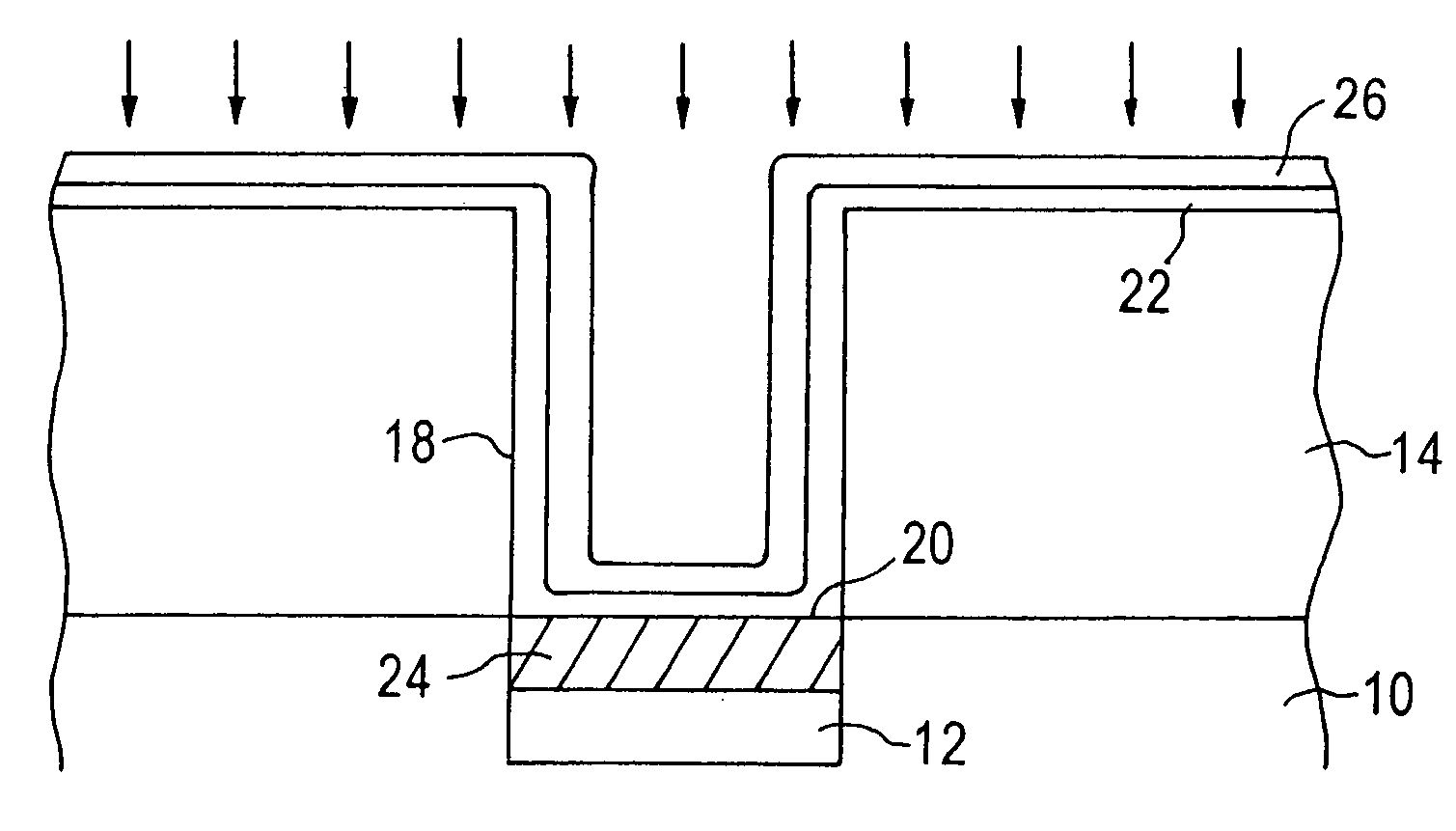
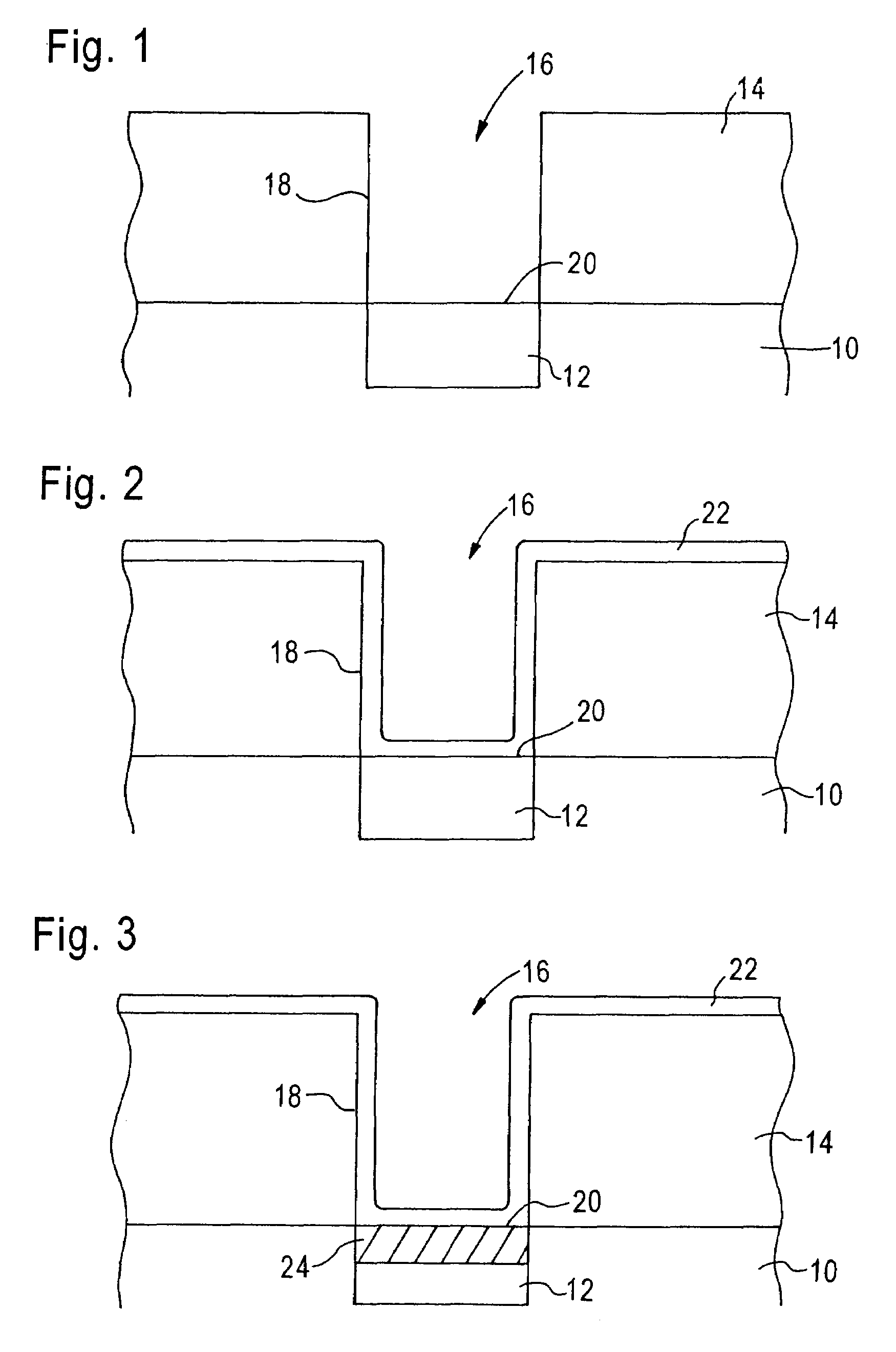
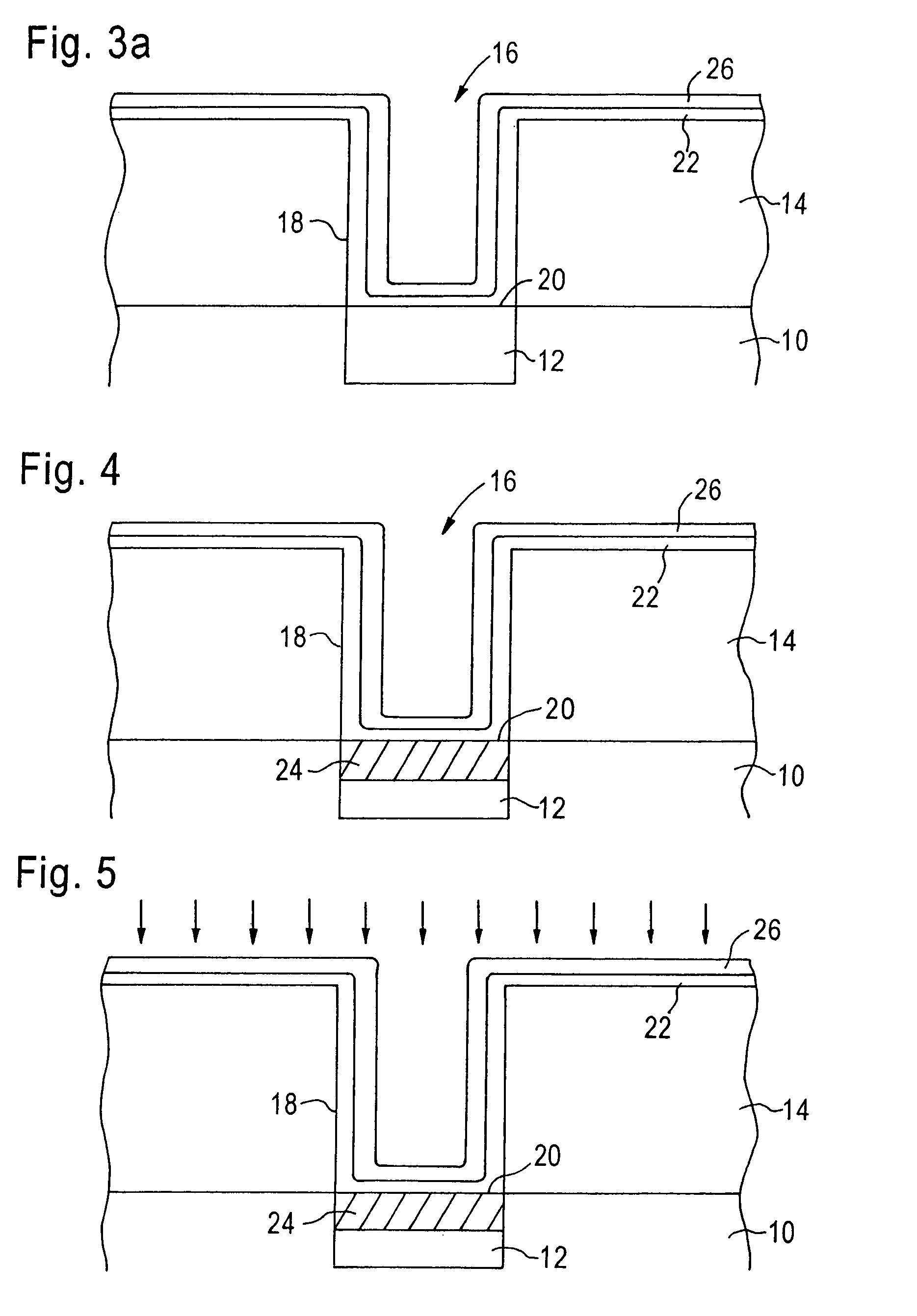
[0021]The present invention addresses and solves problems related to the formation of a contact in a semiconductor device, and particularly to problems arising from the plasma treatment provided to contact barrier metal layers and its effect on the contact metal underneath the barrier metal. This is achieved by the present invention, in part, by the formation of a silicide with a refractory metal contact layer and the conductive region of the substrate, prior to the formation of the contact barrier metal layer. In other embodiments, the contact barrier metal layer is formed on the contact metal, but the plasma treatment is not performed until after formation of the silicide. Hence, when the plasma treatment is performed on the contact barrier metal layer, the titanium silicide has already been formed. This prevents the titanium in the contact metal layer from being prematurely converted to titanium nitride before being able to be converted to titanium silicide.

[0022]FIG. 1 is a sche...


PUM


Abstract

A method of forming a contact in a semiconductor device deposits a refractory metal contact layer in a contact hole on a conductive region portion in a silicon substrate. The refractory metal contact layer is reacted with the silicide region prior to a plasma treatment of a contact barrier metal layer formed within the contact hole. This prevents portions of the refractory metal contact layer from being nitridated prior to conversion to silicide.

Description

FIELD OF THE INVENTION[0001]The present invention relates to the field of semiconductor processing, and more particularly, to the formation of contacts in a metallization process.BACKGROUND OF THE INVENTION[0002]Integrated circuits are manufactured as assemblies of various devices, such as transistors that make up a chip. In the process of manufacturing integrated circuits, after the individual devices, such as transistors, have been fabricated in the silicon substrate, the devices must be connected together to perform the desired circuit functions. This connection process is generally referred to as “metallization”, and is performed using a number of different photolithographic and deposition techniques.[0003]Contact plugs are employed to make a solid connection between an underlying device, for example, and an overlying interconnection conductive line, for example. The fabrication of a contact typically involves forming an opening in the dielectric layer and filling the opening wi...

Claims


Application Information

Patent Timeline
IPC IPC(8): H01L21/4763H01L21/44H01L21/02H01L21/768
CPCH01L21/76843H01L21/76855H01L21/76856
Inventor YU, WENYIN, JINSONGWANG, CONNIE PIN-CHINBESSER, PAULYOSHIE, KEIZABURO
Owner GLOBALFOUNDRIES INC
Why Eureka
Try Eureka