Light emitting element and manufacturing method thereof

a technology of light emitting elements and manufacturing methods, which is applied in the direction of semiconductor devices, basic electric elements, electrical equipment, etc., can solve the problems of increasing the reflectivity of the light emitting surface between the transparent conductor or the translucent electrode and the air space, affecting the light transmission efficiency of the light source, etc., to achieve the effect of suppressing the reduction of light transmissivity, increasing specific resistance, and increasing heat resistan

Inactive Publication Date: 2010-03-23
THE FUJIKURA CABLE WORKS LTD
View PDF15 Cites 10 Cited by
  • Summary
  • Abstract
  • Description
  • Claims
  • Application Information

AI Technical Summary

Benefits of technology

[0024]An object of the present invention is to provide a light emitting device in which the total reflectivity in the light emitting surface formed by the transparent conductor is suppressed and the variation in intensity of light according to direction is little.
[0025]Moreover, another object of the present invention is to provide a compound semiconductor light emitting device in which, by improving the heat resistance of the transparent conductive film, even if annealing is applied in order to achieve the ohmic contact thereof with the metal thin film layer, the transparent conductive film can be kept from being oxidized, the increase in the specific resistance can be suppressed, and the stability of the transmissivity of the transparent conductive film functioning as the window electrode is excellent.
[0031]The manufacturing method of the light emitting device of the second aspect of the present invention is a method of manufacturing a light emitting device, comprising: a laminated body comprising a first conductivity type layer, a second conductivity type layer, and a light emitting portion disposed between the first conductivity type layer and the second conductivity type layer; a metal thin film layer provided on the second conductivity type layer of the laminated body; and a transparent conductor comprising two or more layers of transparent conductive films provided on the metal thin film layer. By changing the thickness of the transparent conductive film serving as an outermost layer in the transparent conductor, the grain size in the light emitting surface of the transparent conductive film is controlled.
[0036]Moreover, in the manufacturing method of the light emitting device according to the first and second aspects of the present invention, by changing the thickness of the transparent conductor, the grain size in the light emitting surface can be controlled, to reduce the variation in the emitting light.
[0038]In particular, since the transparent conductive film serving as the lowest layer is highly conductive and highly transmissive, and the transparent conductive film serving as at least one layer in the upper layer has a higher heat resistance than that of the transparent conductive film serving as the lowest layer, the transparent conductive film serving as the lowest layer can be kept from being oxidized. Together with this, the increase in the specific resistance and the reduction in the light transmissivity can be suppressed.
[0039]Moreover, in the manufacturing method of the light emitting device according to the third aspect of the present invention, since a spray pyrolysis deposition method is used for all of the transparent conductive films constituting the transparent conductor, thin films can be formed in atmospheric air, and a depressurization system is unnecessary. Hence the production cost can be reduced.

Problems solved by technology

Moreover, when an insulative substrate such as sapphire is used, unlike other light emitting devices using a conductive semiconductor substrate such as GaAs and InP, an electrode cannot be provided on the substrate side.
However, in the above gallium nitride compound semiconductor light emitting devices 300, 400, and 500, the refractive index of the transparent conductors 315 and 480 and the translucent electrode 505 is about 2.0, and the refractive index of an air space is about 1.0, thus causing a problem in that, when light emitted in the light emitting layer passes through the transparent conductor or the translucent electrode and emits into the air space, the total reflectivity in the interface (light emitting surface) between the transparent conductor or the translucent electrode and the air space is increased and the intensity of light varies according to the direction.

Method used


Image

  • Light emitting element and manufacturing method thereof
  • Light emitting element and manufacturing method thereof
  • Light emitting element and manufacturing method thereof

Examples


example 1-1

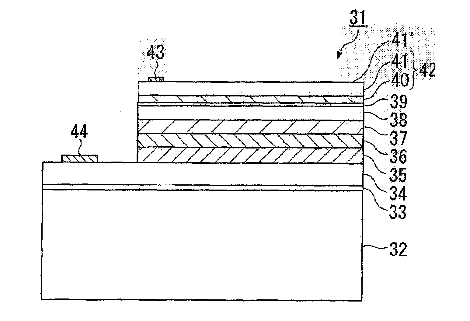
[0056]A wafer was prepared in which on one surface of the sapphire substrate 2 were sequentially laminated the n-type GaN layer 4, the n-type AlGaN layer 5, the light emitting portion 6 having a multiple quantum well (MQW) structure of InGaN and GaN, the p-type AlGaN layer 7, the p-type GaN layer 8, and the metal thin film layer 9 formed from Ni. On this metal thin film layer 9 was formed a transparent conductive film 10 formed from an ITO film having a thickness of 100 nm. The grain size in the surface (light emitting surface 10′) of the transparent conductive film 10 formed from the ITO film was 30 nm.

[0057]Next, on the transparent conductor 12 was formed a mask, and then etching was performed until the periphery of one surface of the n-type GaN layer 4 was exposed. On the exposed n-type GaN layer 4, aluminum was deposited to a thickness of about 0.4 μm, so as to form an n-side electrode 14. On the other hand, on a part of the periphery of the transparent conductor 12 (transparent...

example 1-2

[0059]The light emitting device 1 was produced in the same manner as that of Example 1-1, except that the thickness of the ITO film in Example 1-1 was 320 nm, and the grain size in the light emitting surface was 100 nm.

example 1-3

[0060]The light emitting device 1 was produced in the same manner as that of Example 1-1, except that the thickness of the ITO film in Example 1-1 was 850 nm, and the grain size in the light emitting surface was 200 nm.


PUM


Abstract

A light emitting device having little variation in the intensity of light emitted from the light emitting surface is provided. The light emitting device of exemplary embodiments of the present invention includes a laminated body with a first conductivity type layer and a second conductivity type layer, with a light emitting portion therebetween. The light emitting device also includes a metal thin film layer on the second conductivity type layer of the laminated body, and a transparent conductor on the metal thin film layer. The transparent conductor includes a single layer of transparent conductive film. The grain size in the light emitting surface of the transparent conductive film is not less than 30 nm and not greater than 300 nm.

Description

CROSS-REFERENCE TO RELATED APPLICATIONS[0001]This application claims priority from PCT Application No. PCT / JP2005 / 013698, filed Jul. 27, 2005; and from Japanese Patent Application Nos. 2004-223980, 2004-223981, and 2004-223982, filed Jul. 30, 2004; and from Japanese Patent Application No. 2005-201581, filed Jul. 11, 2005, the contents of which are incorporated herein in their entirety by reference.BACKGROUND OF THE INVENTION[0002]1. Field of the Invention[0003]Apparatuses and methods consistent with the present invention relate to a compound semiconductor light emitting device for obtaining light from a compound semiconductor layer, and more particularly, to a compound semiconductor light emitting device which uses a transparent conductive film as a window electrode.[0004]2. Description of the Related Art[0005]Gallium nitride compound semiconductors, such as GaN, AlGaN, InGaN, and InGaAlN, are drawing attention as visible light emitting devices of green, blue, or the like.[0006]In t...

Claims


Application Information

Patent Timeline
Patent Type & Authority Patents(United States)
IPC IPC(8): H01L27/15H01L33/42
CPCH01L33/42
Inventor GOTO, KENJIKAWASHIMA, TAKUYATANABE, NOBUOITO, TATSUYA
Owner THE FUJIKURA CABLE WORKS LTD
Why Eureka
Try Eureka