Electro-optic modulator
a modulator and optical technology, applied in the field of optical modulators, can solve the problems of adversely affecting the performance of the device and its reproducibility, and achieve the effect of reducing unwanted electrical effects and clearly defined doped regions
- Summary
- Abstract
- Description
- Claims
- Application Information
AI Technical Summary
Benefits of technology
Problems solved by technology
Method used
Image
Examples
first embodiment
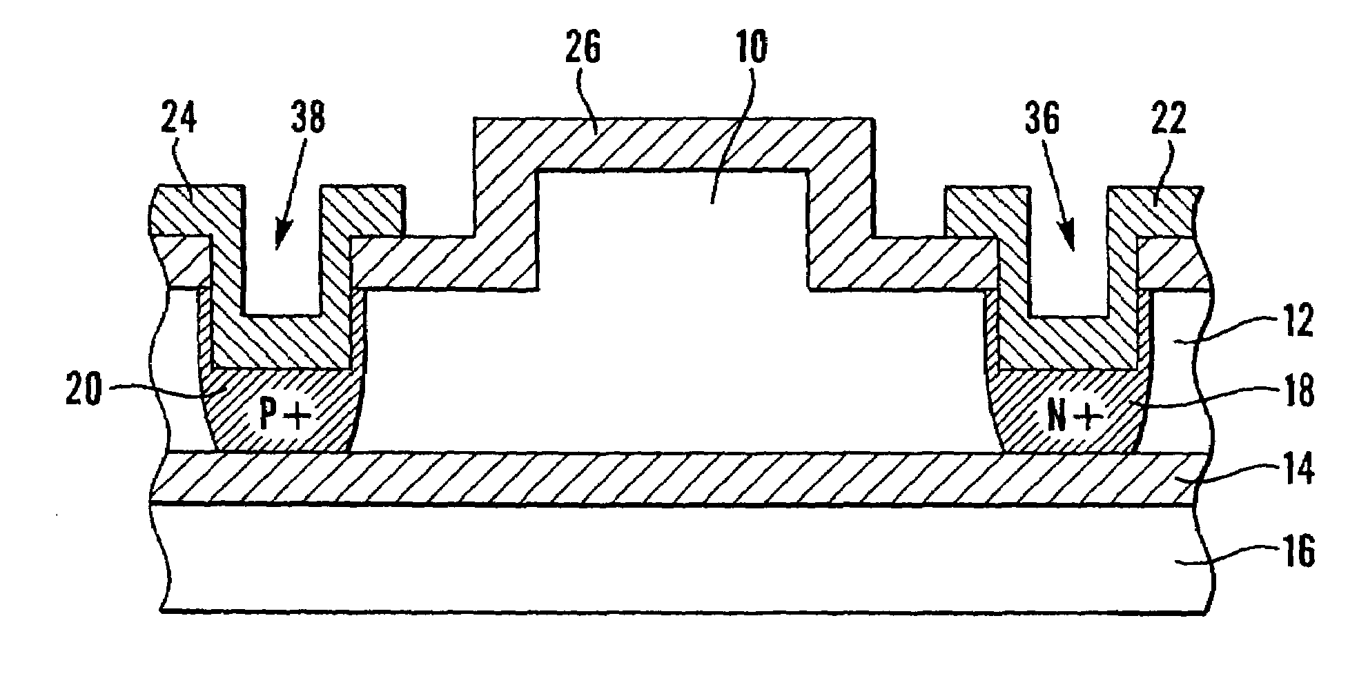
[0032]FIG. 3 shows the invention. The rib waveguide 10 is again formed on the silicon epi layer 12 of the SOI structure. However, a pair of trenches 36, 38 are formed either side of the rib waveguide 10 and doping is carried out into these trenches to form an n+ doped area 18 and a p+ doped area 20. Metal contacts 22, 24 are again provided, as is a protective and insulating oxide layer 26.
[0033]The increased depth from which the doping is carried out, due to the trenches 36, 38, means that the n+ and p+ doped areas 18, 20 reach the insulating layer 14 beneath the silicon epi layer 12.
[0034]FIG. 4 shows a similar structure according to a second embodiment of the invention. In the first embodiment of FIG. 3, doping is carried out so as to extend from the base of the recesses 36, 38 only. In FIG. 4, this limitation of the extent of doping is not present. These examples could be achieved (for example) by diffusion processes or by ion implantation. In FIG. 3, the protective oxide layer 2...
third embodiment
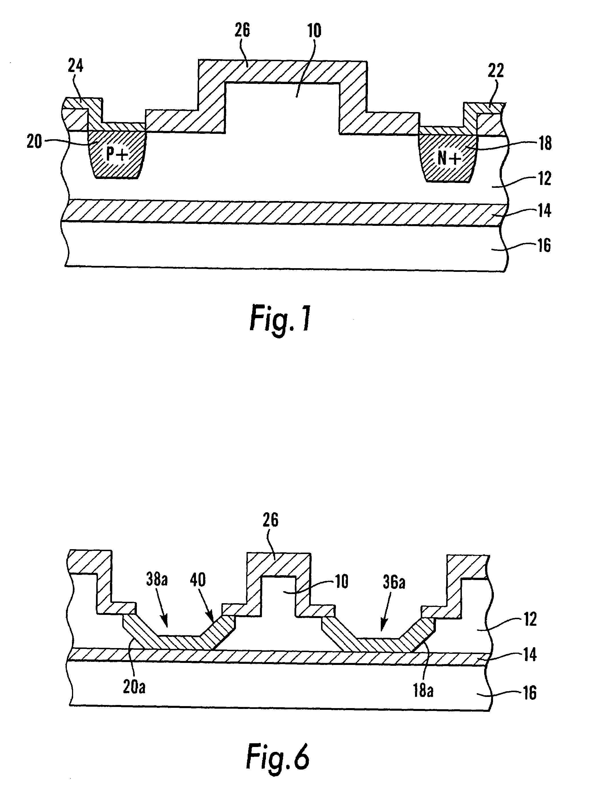
[0038]FIG. 6 shows the present invention. This corresponds generally to that of FIG. 4 but the trench recesses 36a, 38a are formed with angled edges such as that at 40. This can be achieved via a v-groove etch, for example. This eases the deposition of the metal contacts (not shown in FIG. 6) as they do not need to traverse a sharp corner and are therefore less prone to thinning. Dopant can be confined to the base of the trench if desired.
[0039]In order to compare the performance advantage by employing the present invention, a device was fabricated according to FIG. 6 with a 1.8 micron etch on a 2.6 micron slab. A second device was fabricated identically except that the diodes were placed on the surface of the slab region as per FIG. 1. Doping was introduced into both devices using a diffusion process, thus creating two structures which are identical except that the vertical depth of the doping is greater in the novel device.
[0040]The attenuation of light passing through the wavegui...
PUM
| Property | Measurement | Unit |
|---|---|---|
| refractive index | aaaaa | aaaaa |
| carrier concentration | aaaaa | aaaaa |
| charge | aaaaa | aaaaa |
Abstract
Description
Claims
Application Information


