III-nitride materials including low dislocation densities and methods associated with the same

a technology of nitride and dislocation density, which is applied in the direction of polycrystalline material growth, crystal growth process, chemically reactive gas growth, etc., can solve the problems of device performance, electrical performance, and dislocation formation of defects,

Active Publication Date: 2010-03-30
MACOM TECH SOLUTIONS HLDG INC
View PDF95 Cites 22 Cited by
  • Summary
  • Abstract
  • Description
  • Claims
  • Application Information

AI Technical Summary

Problems solved by technology

Thus, when III-nitride materials are formed on such substrates, these differences may lead to the formation of defects including dislocations.
The presence of dislocations in III-nitride materials that are in the vicinity of the active region in a device can impair device performance.
For example, the dislocations can function as scattering centers which effect electron transport and, thus, impair electrical performance.
Also, the dislocations can function as non-radiative recombination centers which reduce performance of opto-electronic devices.
Furthermore, dislocations can lead to inhomogeneities in composition and formation of macro-defects which can also negatively effect device performance.
Lateral growth processes are typically more complex than vertical growth processes.

Method used


Image

  • III-nitride materials including low dislocation densities and methods associated with the same
  • III-nitride materials including low dislocation densities and methods associated with the same
  • III-nitride materials including low dislocation densities and methods associated with the same

Examples


example 1

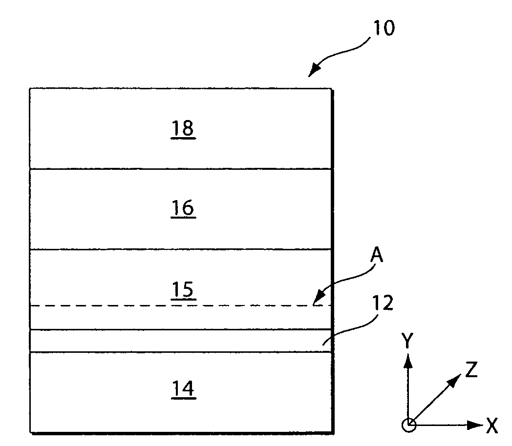
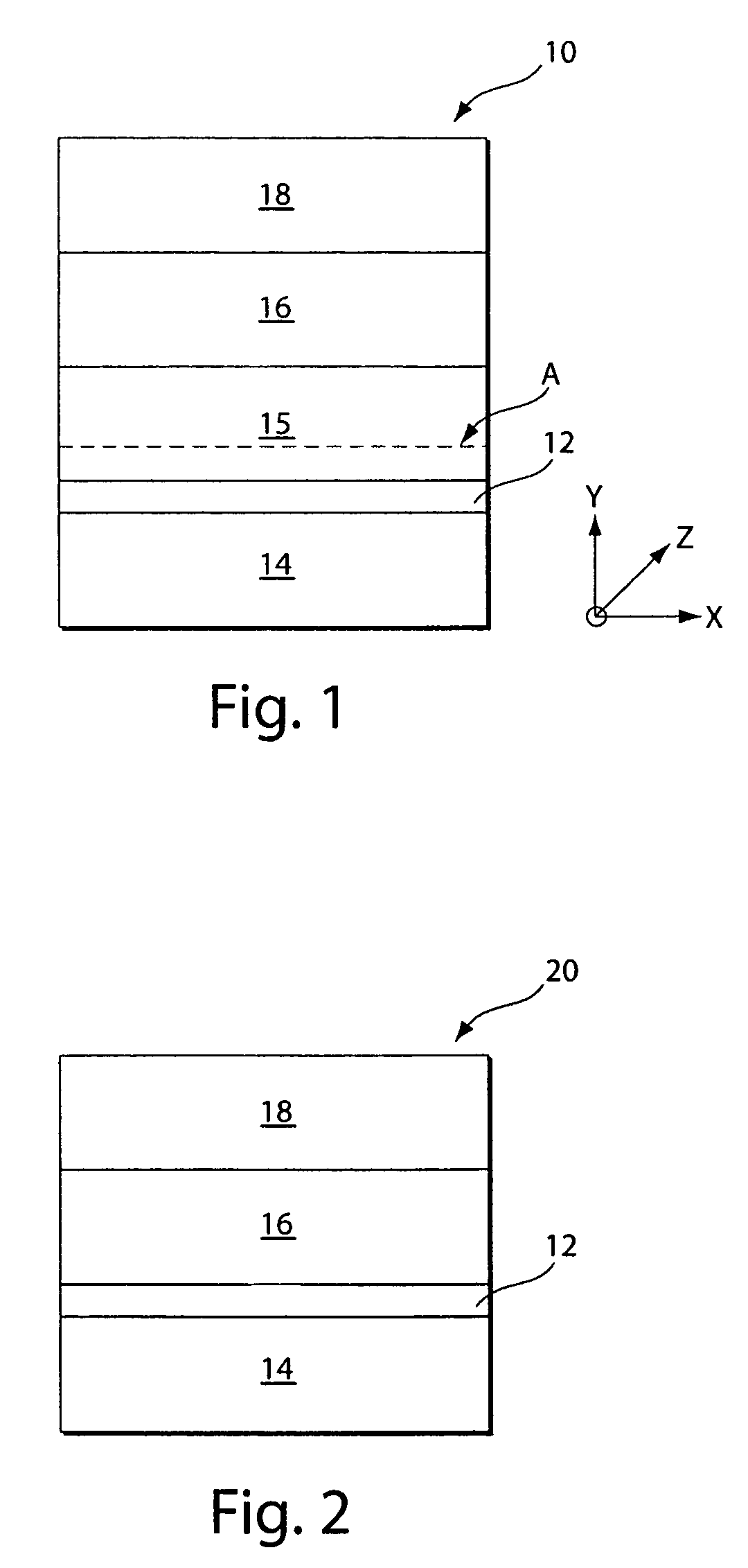
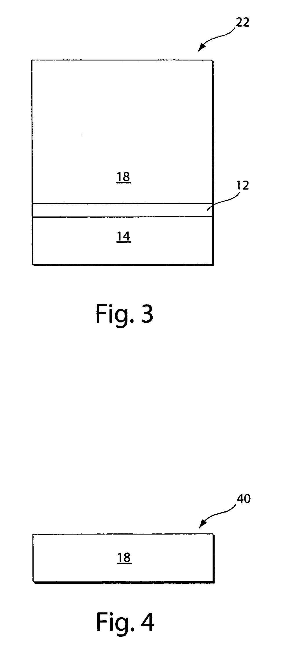
[0123]This example illustrates the formation of a structure including III-nitride material layers / regions having low screw dislocation densities according to one embodiment of the present invention.

[0124]A 100 mm silicon substrate was placed in a reaction chamber. Ammonia gas was introduced into the chamber as a nitrogen source. The temperature was maintained at 1030° C. and the pressure at about 30 torr. A strain-absorbing layer of amorphous silicon nitride (SiN) was formed.

[0125]About 6 seconds after the introduction of ammonia, TMA was introduced into the chamber as an aluminum source. The temperature and pressure were respectively maintained at 1030° C. and about 30 torr. Growth proceeded for about 60 minutes. An aluminum nitride (AlN) was formed.

[0126]After about 60 minutes, TMG was introduced into the chamber. Growth proceeded for about 40 minutes. An aluminum gallium nitride layer (Al0.6Ga0.4N) was formed.

[0127]After about 40 minutes, the concentration of TMG being introduced...


PUM

PropertyMeasurementUnit
thicknessaaaaaaaaaa
areaaaaaaaaaaa
thicknessaaaaaaaaaa

Abstract

Semiconductor structures including one, or more, III-nitride material regions (e.g., gallium nitride material region) and methods associated with such structures are provided. The III-nitride material region(s) advantageously have a low dislocation density and, in particular, a low screw dislocation density. In some embodiments, the presence of screw dislocations in the III-nitride material region(s) may be essentially eliminated. The presence of a strain-absorbing layer underlying the III-nitride material region(s) and / or processing conditions can contribute to achieving the low screw dislocation densities. In some embodiments, the III-nitride material region(s) having low dislocation densities include a gallium nitride material region which functions as the active region of the device. The low screw dislocation densities of the active device region (e.g., gallium nitride material region) can lead to improved properties (e.g., electrical and optical) by increasing electron transport, limiting non-radiative recombination, and increasing compositional / growth uniformity, amongst other effects.

Description

FIELD OF INVENTION[0001]The invention relates generally to III-nitride materials and, more particularly, to III-nitride (e.g., gallium nitride) material structures including low dislocation densities, as well as methods associated with the same.BACKGROUND OF INVENTION[0002]III-nitride materials include gallium nitride (GaN), aluminum nitride (AlN), indium nitride (InN) and their respective alloys (e.g., AlGaN, InGaN, AlInGaN and AlInN). In particular, gallium nitride materials (GaN and its alloys) have attractive properties including the ability to efficiently emit blue light, the ability to transmit signals at high frequency, and others. Accordingly, gallium nitride materials are being widely investigated in many microelectronic applications such as transistors, field emitters, and optoelectronic devices. Semiconductor structures that include gallium nitride material regions oftentimes include regions of other III-nitride materials (e.g., AlN). Such layers, for example, may functio...

Claims


Application Information

Patent Timeline
Patent Type & Authority Patents(United States)
IPC IPC(8): H01L31/101C30B25/02C30B29/40H01L21/20H01L33/00
CPCC30B25/02C30B29/403H01L21/02381H01L21/02458H01L21/02543H01L21/02505H01L21/0251H01L21/02513H01L21/0254H01L21/02488
Inventor PINER, EDWIN L.ROBERTS, JOHN C.RAJAGOPAL, PRADEEP
Owner MACOM TECH SOLUTIONS HLDG INC
Why Eureka
Try Eureka