Semiconductor structure comprising active zones

Inactive Publication Date: 2010-04-06
AZUR SPACE SOLAR POWER
View PDF12 Cites 204 Cited by
  • Summary
  • Abstract
  • Description
  • Claims
  • Application Information

AI Technical Summary

Benefits of technology

[0010]On the basis of this as prior art, the object of the present invention is to further develop a semiconductor structure with active zones and a method for manufacturing such a structure, with which the disadvantages of the prior art can be eliminated. Especially, a light-emittin

Problems solved by technology

Thus its use in a colo

Method used


Image

  • Semiconductor structure comprising active zones
  • Semiconductor structure comprising active zones
  • Semiconductor structure comprising active zones

Examples


Example

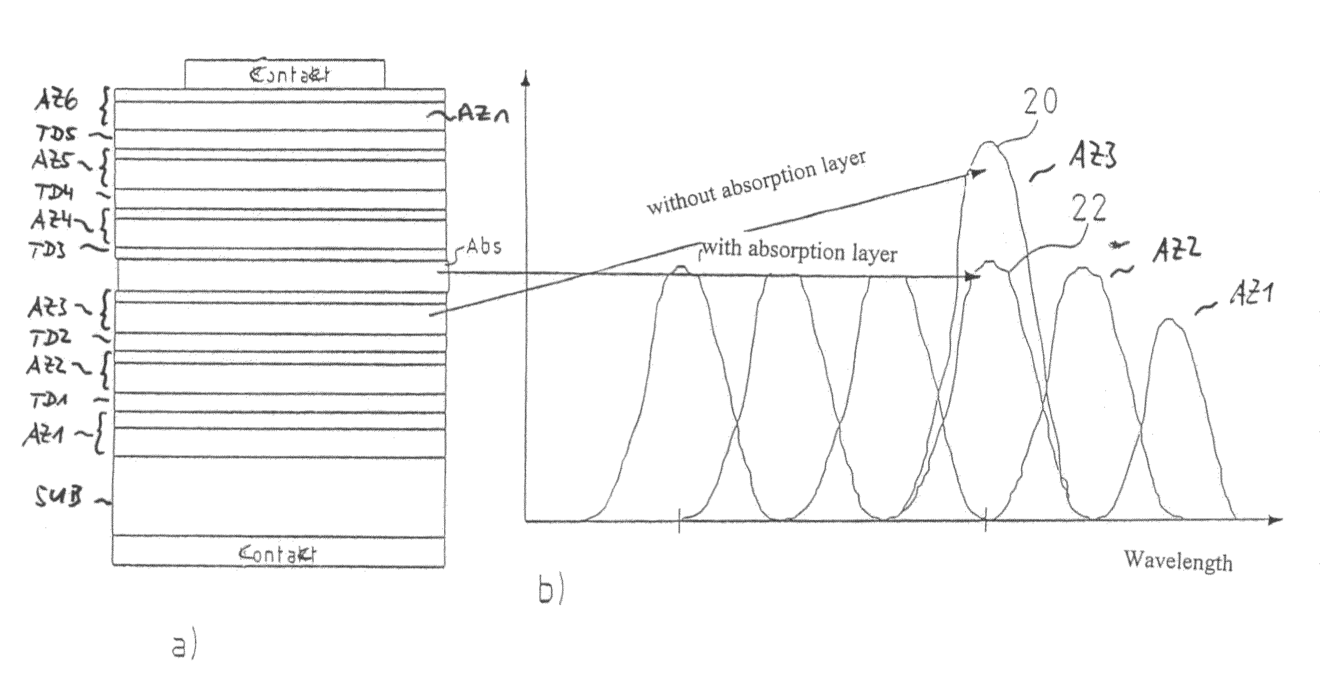
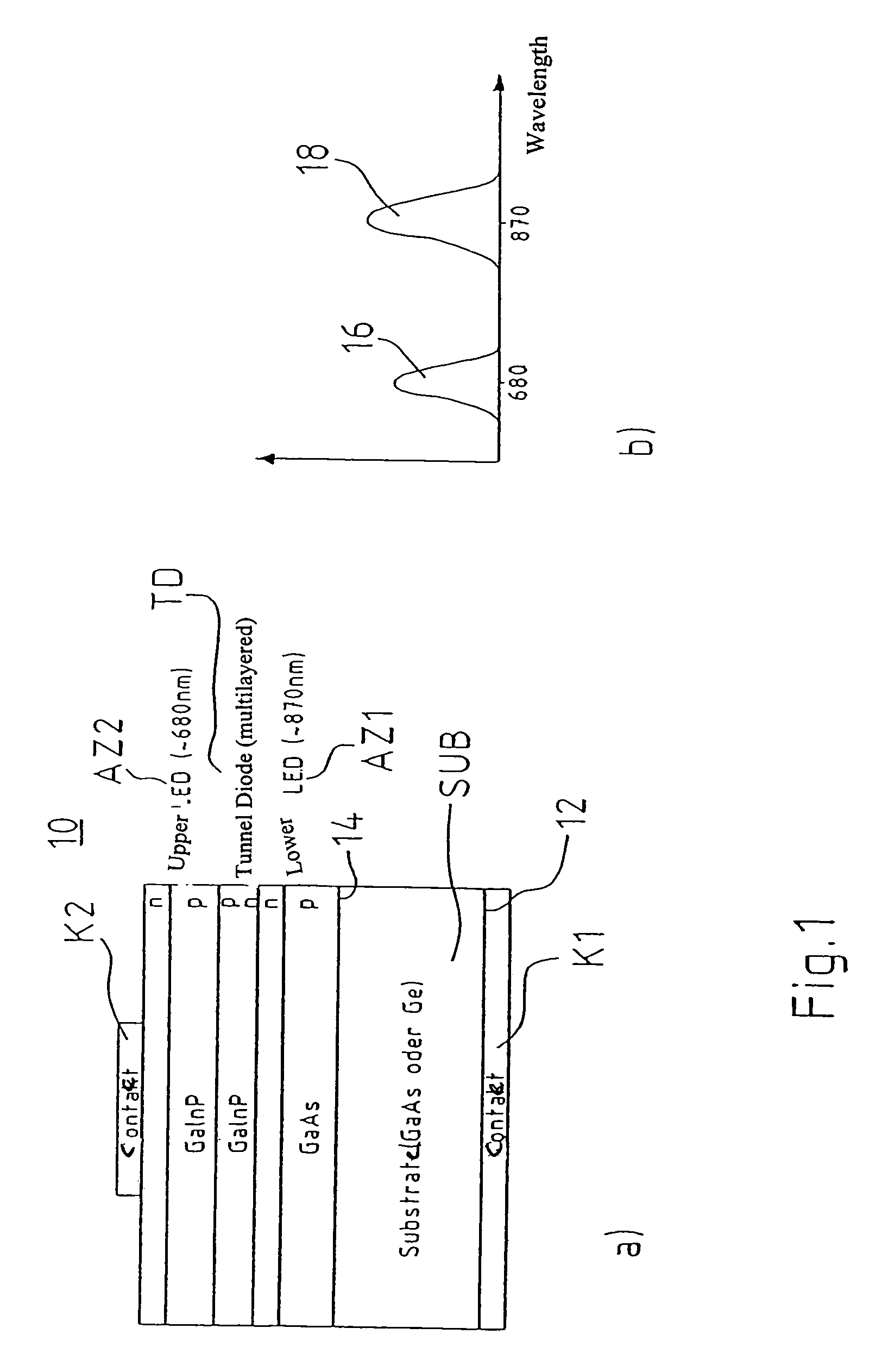
[0060]FIG. 1 shows a schematic configuration of a semiconductor structure 10 with active zones AZ, which structure can be characterized as a two-peak light-emitting diode. The two-peak diode 10 comprises a substrate SUB, which is made, for example, of GaAs or Ge material. A lower surface 12 of the substrate SUB is provided with a metallic contact K1, and a first (lower) active zone AZ1 is grown on an upper surface 14 as, for example, a GaAs diode. Above the lower active zone AZ1 a dividing layer TD1 is arranged as an isolation diode, for example a GaInP isolation diode, the thickness of which is approximately 40 nm. This isolation diode TD serves and acts as a low-impedance interconnect resistor for the serial connection of the lower active zones AZ1, which are designed as pn junctions. Above the tunnel diode TD, another, upper active zone AZ2 is grown, which is designed, for example, as a GaInP diode. FIG. 1b shows an exemplary spectral distribution, wherein a first peak 16 lies wi...


PUM


Abstract

A semiconductor structure with active zones, such as light diodes or photodiodes, including a substrate (SUB) with at least two active zones (AZ1-AZn), each of which emits or absorbs a radiation of differing wavelength. According to the invention, a multi-wavelength diode may be achieved, in which a first (lower) active zone (AZ1) is grown on a surface of the substrate (SUB), with one or several further active zones (AZ1-Azn) epitaxially grown one on the other and the active zones (AZ1-AZn) are serially connected from the lower active zone (AZ1) to an upper active zone (AZn), by means of tunnel diodes (TD1-TDn), serving as low-impedance resistors.

Description

[0001]This application is a filing under 35 USC 371 of PCT / EP2005 / 000759, filed Jan. 26, 2005.BACKGROUND OF THE INVENTION[0002]The invention relates to a semiconductor structure with active zones, and to a method for manufacturing such a semiconductor. The invention further relates to a blended-color sensor, and to a colored display that contains the semiconductor structure with the active zones.[0003]A semiconductor structure with active zones of the type mentioned above is described in an article by I. Ozden, et al.: “A dual-wavelength indium gallium nitride quantum well light emitting diode” in Applied Physics Letters, Vol. 79, No. 16, 2001, pp 2532-2534. This article deals with a monolithic, dual wavelength (blue / green) light-emitting diode (LED) with two active indium-gallium-nitride / gallium nitride (InGaN / GaN) multiple quantum well segments. The segments are part of a single vertical epitaxial structure, in which a p++ / n++ / InGaN / GaN tunnel junction is inserted between the LED'...

Claims


Application Information

Patent Timeline
IPC IPC(8): H01L33/00H01L27/15H01L33/08H01L31/0304H01L31/109H01L31/11
CPCH01L25/0756H01L27/15H01L31/109H01L31/11H01L33/08H01L2224/48463H01L2924/3011H01L2924/00
Inventor BENSCH, WERNER
Owner AZUR SPACE SOLAR POWER
Why Eureka
Try Eureka