Semiconductor device including a crystal semiconductor layer, its fabrication and its operation

a semiconductor layer and semiconductor technology, applied in the direction of transistors, crystal growth processes, chemistry apparatus and processes, etc., can solve the problems of deterioration of many other characteristics of semiconductor devices, inconvenient processing, complicated and inconvenient processes,

Active Publication Date: 2010-04-13
SAMSUNG ELECTRONICS CO LTD
View PDF13 Cites 117 Cited by
  • Summary
  • Abstract
  • Description
  • Claims
  • Application Information

AI Technical Summary

Problems solved by technology

Consequently, the trends result in a deterioration of many other characteristics of semiconductor devices, such as high speed, low power consumption, and the like, though these properties continue to be in increasing demand.
A main drawback, however, of the first method is that its processes are complicated and inconvenient because a LOCOS process or an STI process must be performed to form an isolation layer after oxygen ions are implanted into a silicon substrate, and a thermal treatment process is performed.
Furthermore, serious defects may be generated inside the semiconductor substrate on which elements will be formed.
In the second method, however, since two substrates having an insulating layer formed thereon are attached at a high temperature, and one side of the substrates is polished, it is required to perform a thermal treatment process at a high temperature, and voids may be generated at the junction portion of the substrates.
However, a continuous effort is required to fabricate an improved semiconductor device using a crystalline semiconductor layer formed on the semiconductor substrate as well as to form the SOI substrate.

Method used


Image

  • Semiconductor device including a crystal semiconductor layer, its fabrication and its operation
  • Semiconductor device including a crystal semiconductor layer, its fabrication and its operation
  • Semiconductor device including a crystal semiconductor layer, its fabrication and its operation

Examples


Embodiment Construction

[0039]The present invention will now be described more fully hereinafter with reference to the accompanying drawings, in which preferred embodiments of the invention are shown. This invention may, however, be embodied in many different forms and should not be construed as being limited to the embodiments set forth herein. Rather, these embodiments are provided so that this disclosure will be thorough and complete, and will fully convey the scope of the invention to those skilled in the art. In the drawings, the thicknesses of layers and regions are exaggerated for clarity. Like numbers refer to like elements throughout the specification.

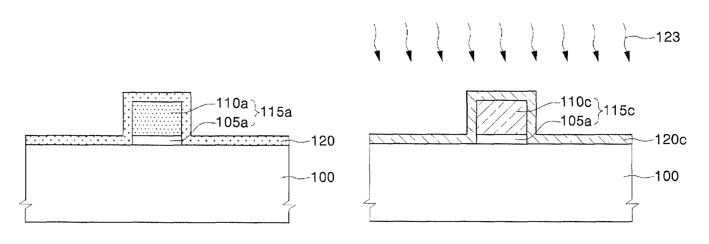
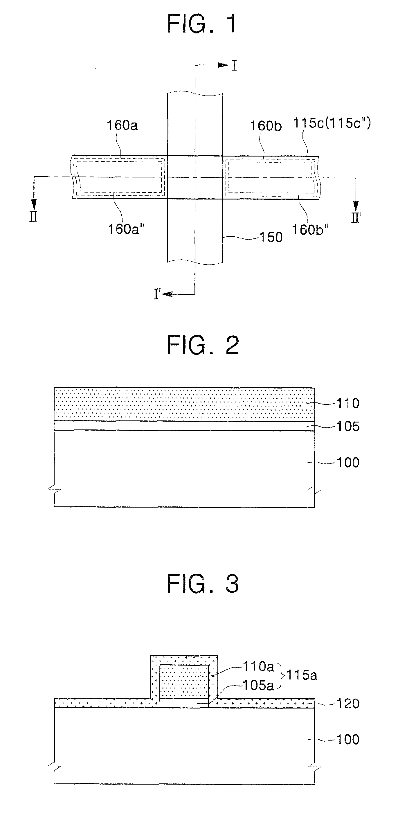
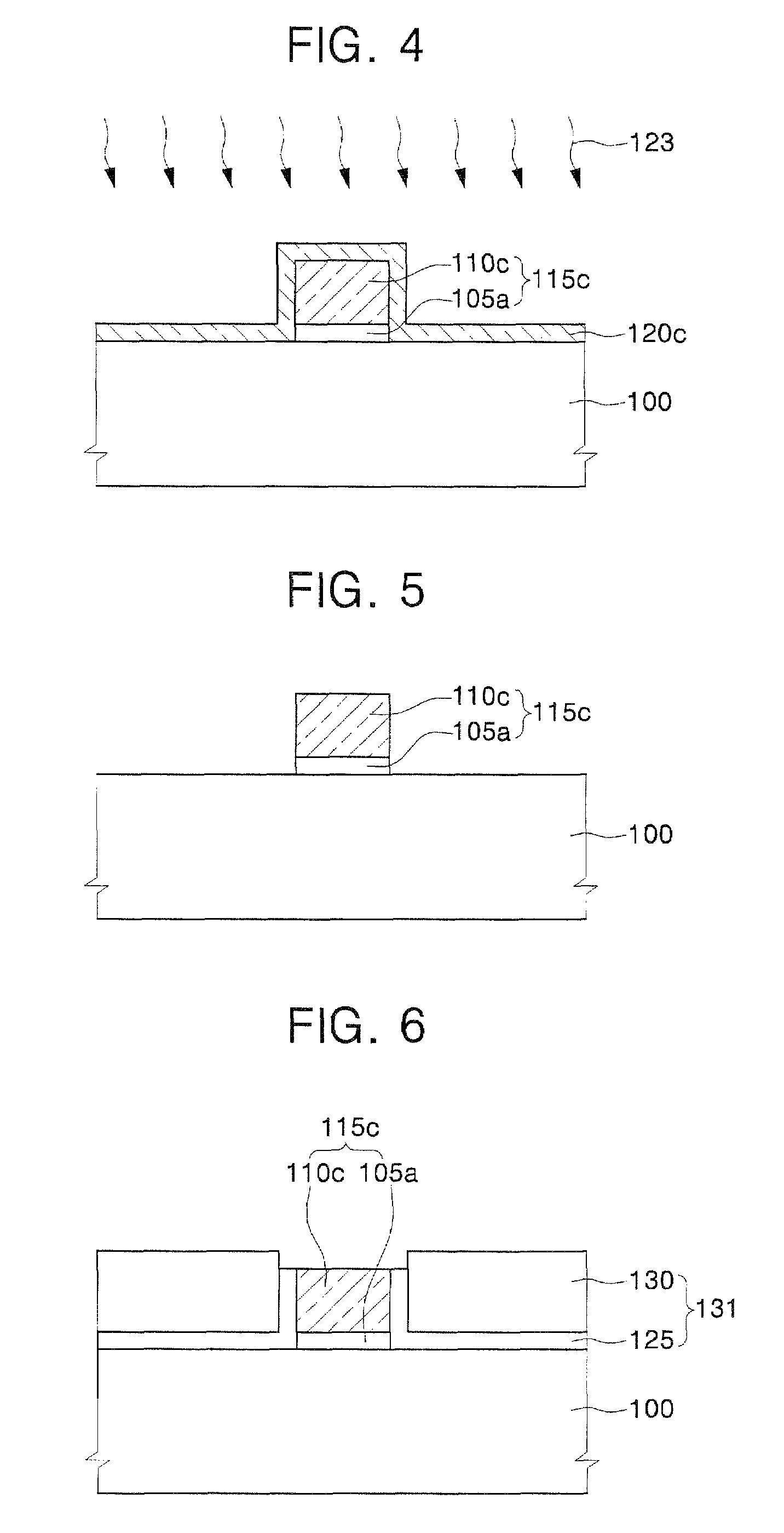
[0040]FIG. 1 is a plan view illustrating a semiconductor device according to an embodiment of the present invention, and FIGS. 2 through 7 are cross-sectional views taken along line I-I′ of FIG. 1 illustrating a method of fabricating a semiconductor device according to some embodiments of the present invention.

[0041]Referring to FIGS. 1 and 2, a semi...


PUM


Abstract

In one embodiment, a method of fabricating a semiconductor device having a crystalline semiconductor layer includes preparing a semiconductor substrate and forming a preliminary active pattern on the semiconductor substrate. The preliminary active pattern includes a barrier pattern and a non-single crystal semiconductor pattern. A sacrificial non-single crystal semiconductor layer covers the preliminary active pattern and the semiconductor substrate. By crystallizing the sacrificial non-single crystal semiconductor layer and the non-single crystal semiconductor pattern, using the semiconductor substrate as a seed layer, the sacrificial non-single crystal semiconductor layer and the non-single crystal semiconductor pattern are changed to a sacrificial crystalline semiconductor layer and a crystalline semiconductor pattern, respectively. The crystalline semiconductor pattern and the barrier pattern constitute an active pattern. The sacrificial crystalline semiconductor layer is removed.

Description

CROSS-REFERENCE TO RELATED APPLICATION[0001]This application claims priority from Korean Patent Application No. 2005-0110986, filed Nov. 18, 2005, the disclosure of which is hereby incorporated herein by reference in its entirety as if set forth fully herein.BACKGROUND OF INVENTION[0002]1. Technical Field[0003]The present invention relates to a semiconductor device, a fabricating method thereof, and an operating method thereof, and more particularly, to a semiconductor device having a crystalline semiconductor layer, a fabricating method thereof, and an operating method thereof.[0004]2. Discussion of the Related Art[0005]With a highly integrated semiconductor device, channel lengths of transistors and distances, such as between transistors, are small. And as integration increases, those sizes and distances become smaller. Also, one will find with recent trends that concentrations of impurities in semiconductor substrates have increased, and thus, source / drain junction capacitances o...

Claims


Application Information

Patent Timeline
Patent Type & Authority Patents(United States)
IPC IPC(8): H01L21/20H01L21/36
CPCH01L27/108H01L27/10802H01L29/785H01L29/66795H01L21/2026H01L27/10879H01L27/10826H01L21/02488H01L21/02502H01L21/02496H01L21/02505H01L21/02675H01L21/02491H01L21/02598H01L21/02532H01L21/0245H01L21/02513H01L21/02378H01L21/02381H01L21/02447H10B12/20H10B12/36H10B12/056H10B12/00H01L29/1033H01L21/02639H01L21/02667
Inventor KIM, SUNG-MINYUN, EUN-JUNG
Owner SAMSUNG ELECTRONICS CO LTD
Why Eureka
Try Eureka