Electron device and process of manufacturing thereof

Inactive Publication Date: 2010-04-13
FUJITSU LTD +1
View PDF19 Cites 2 Cited by
  • Summary
  • Abstract
  • Description
  • Claims
  • Application Information

AI Technical Summary

Benefits of technology

[0006]An object of the present invention is to provide an electron device which has a fine structure, which operates extremely stably at room temperature, which can be mass produced inexpensively by utilizing pho

Problems solved by technology

However, when the capacity of the capacitor electrodes is extremely small (e.g., about 10−18 farads), the change in the static electric potential, which arises due to one electron tunneling, greatly

Method used


Image

  • Electron device and process of manufacturing thereof
  • Electron device and process of manufacturing thereof
  • Electron device and process of manufacturing thereof

Examples


Example

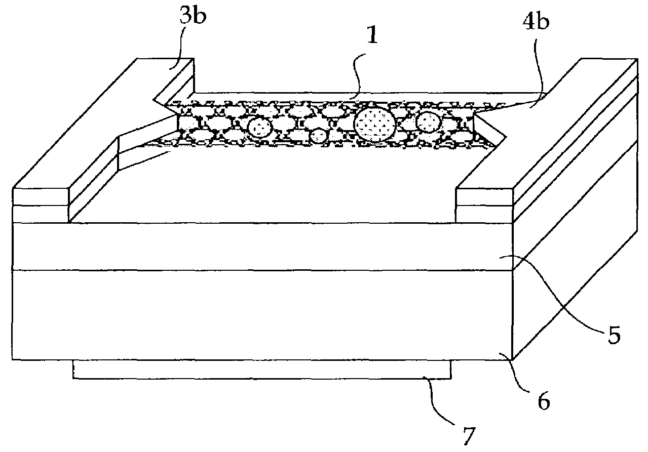
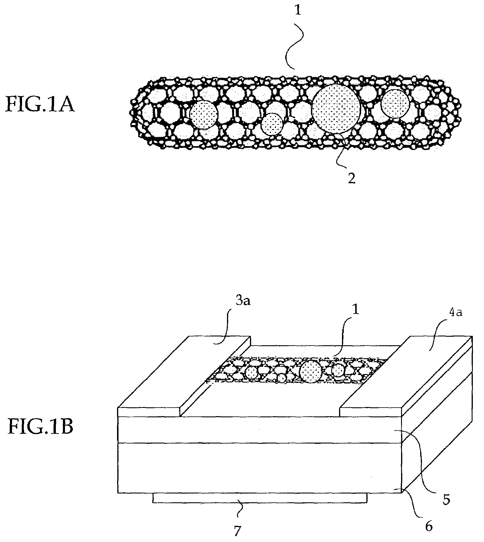
[0020]The electron device of the present invention has a carbon-based linear structural body including at least one conductive particle; and a first electrode and a second electrode which are disposed such that at least one conductive particle included in the carbon-based linear structural body is disposed between the first electrode and the second electrode. As needed, the electron device may also have a third electrode which imparts an electric field effect to the carbon-based linear structural body, and other members. The term “electron device” of the present invention refers to devices such as electron devices, semiconductor devices, single electron semiconductor devices and the like.

[0021]The carbon-based linear structural body is not particularly limited as long as it has a structure in which a plurality of tunnel junctions are connected in series at the interior thereof, and can be appropriately selected in accordance with the object. Suitable examples include a carbon-based ...


PUM


Abstract

The electron device of the present invention has a carbon-based linear structural body including at least one conductive particle, a first electrode and a second electrode disposed at both end of the carbon-based linear structural body, so as to subject the carbon-based linear structural body including at least one conductive particle to connect between the first electrode and the second electrode. A process of manufacturing the electron device includes steps of: forming a carbon-based linear structural body including at least one conductive particle, using a catalyst of a first island and a second island selected from two or more of islands of the catalyst on a substrate; and forming a first electrode and a second electrode so as to connect the first electrode with the first island and one end of the carbon-based linear structural body, and the second electrode with the second island and the other end of the carbon-based linear structural body.

Description

CROSS-REFERENCE TO RELATED APPLICATIONS[0001]This application is based upon and claims the benefits of the priority from the prior Japanese Patent Application No. 2002-144905, filed in May 20, 2002, the entire contents of which are incorporated herein by reference.BACKGROUND OF THE INVENTION[0002]1. Field of the Invention[0003]The present invention relates to an electron device, which is suitable for single electron transistors utilizing carbon nanotubes which are self-organizing nanostructures, and to an efficient process of manufacturing the electron device.[0004]2. Description of the Related Art[0005]A single electron transistor is a three-terminal element utilizing the single electron effect. The single electron effect is also called the Coulomb blockade effect, and this effect is based on a phenomenon derived from the fact that there exists no smaller quantity of electricity than the unit electric charge amount of an electron. When a capacitor is made to approach the nanometer ...

Claims


Application Information

Patent Timeline
IPC IPC(8): H01L29/12H01L29/06H01L29/66H01L29/786H01L51/30
CPCB82Y10/00H01L51/0046H01L51/0048H01L51/0545Y10S977/745Y10S977/748Y10S977/749H10K85/211H10K85/221H10K10/466
Inventor AWANO, YUJIMATSUMOTO, KAZUHIKO
Owner FUJITSU LTD
Why Eureka
Try Eureka