Tunneling effect transistor with self-aligned gate

a technology of tunneling effect transistor and gate, which is applied in the direction of semiconductor devices, semiconductor/solid-state device details, diodes, etc., can solve the problems of degrading device performance as an electronic switch, large substrate area, and inability to integrate into practical products

Active Publication Date: 2010-04-20
TWITTER INC
View PDF3 Cites 121 Cited by
  • Summary
  • Abstract
  • Description
  • Claims
  • Application Information

AI Technical Summary

Problems solved by technology

While demonstrating such favorable device characteristics, currently known tunneling effect transistors are not suitable for integration into practical products due to low drive current per unit area compared with conventional field effect transistors.
In general, prior art tunneling effect transistors do not provide self-alignment, which results in a large footprint on a substrate area.
Further, the large footprint is unavoidably associated with a large parasitic capacitance, further degrading device performance as an electronic switch.
Thus, the gate cannot have a sublithographic length, which becomes a limiting factor in scaling this prior art device.
Further, reduction of input capacitance of this prior art device is necessarily limited by the relatively large physical size.
However, this prior art structure requires many epitaxial silicon deposition steps, which is difficult to incorporate into standard complementary metal oxide semiconductor (CMOS) processing steps.
Manufacturing of this structure requires many epitaxial silicon deposition steps, which may not be easily integrated into standard CMOS processing sequences.

Method used


Image

  • Tunneling effect transistor with self-aligned gate
  • Tunneling effect transistor with self-aligned gate
  • Tunneling effect transistor with self-aligned gate

Examples


Embodiment Construction

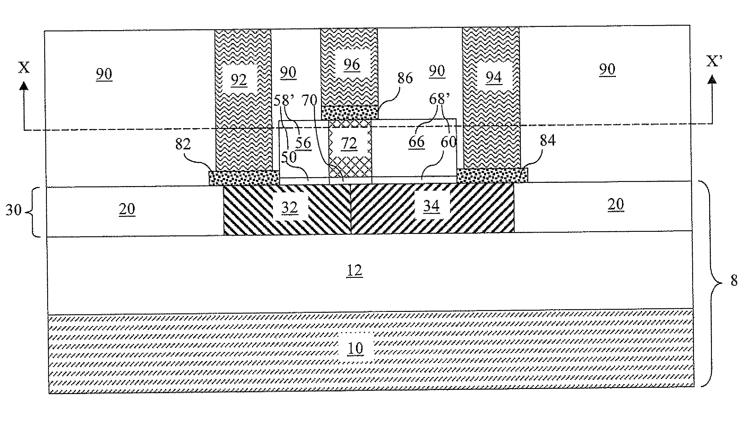
[0075]As stated above, the present invention relates to tunneling effect transistor structures having a self-aligned gate and methods of manufacturing the same, which are now described in detail with accompanying figures. It is noted that like and corresponding elements are referred to by like reference numerals.

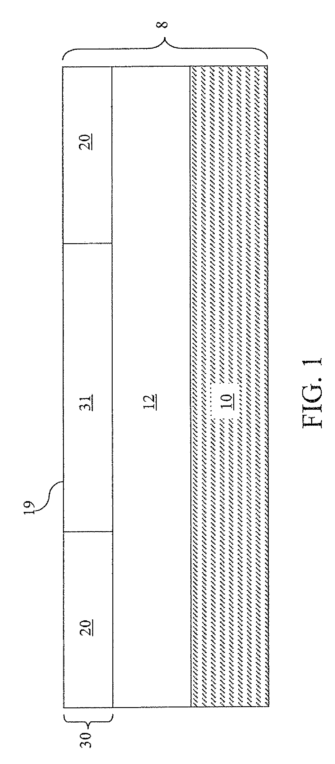
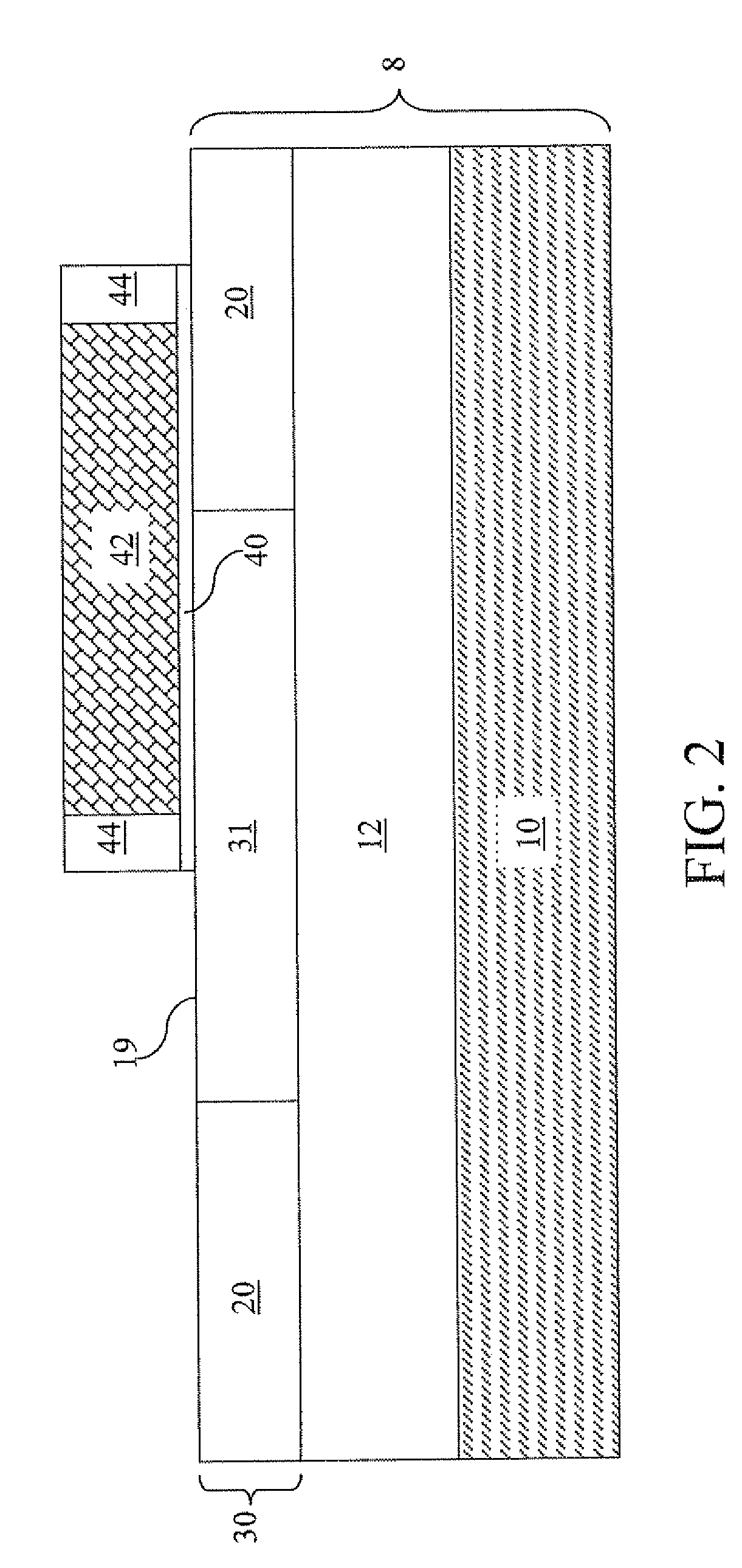
[0076]Referring to FIG. 1, a first exemplary semiconductor structure according to one embodiment of the present invention comprises a semiconductor substrate 8 having a handle substrate 10, a buried insulator layer 12, and a top semiconductor layer 30. The top semiconductor layer 30 contains a semiconductor region 31 and shallow trench isolation 20. The thickness of the top semiconductor layer 30 may be from about 20 nm to about 300 nm, although lesser and greater thickness are herein contemplated also. Methods of forming the shallow trench isolation 20 which comprises a dielectric material are well known in the art. The shallow trench isolation 20 may comprise a dielectric ...


PUM


Abstract

In one embodiment, a mandrel and an outer dummy spacer may be employed to form a first conductivity type region. The mandrel is removed to form a recessed region wherein a second conductivity type region is formed. In another embodiment, a mandrel is removed from within shallow trench isolation to form a recessed region, in which an inner dummy spacer is formed. A first conductivity type region and a second conductivity region are formed within the remainder of the recessed region. An anneal is performed so that the first conductivity type region and the second conductivity type region abut each other by diffusion. A gate electrode is formed in self-alignment to the p-n junction between the first and second conductivity regions. The p-n junction controlled by the gate electrode, which may be sublithographic, constitutes an inventive tunneling effect transistor.

Description

FIELD OF THE INVENTION[0001]The present invention relates to semiconductor devices, and particularly to tunneling effect transistor structures having a self-aligned gate and methods of manufacturing the same.BACKGROUND OF THE INVENTION[0002]A tunneling effect transistor is essentially a gated tunnel diode. The tunneling effect transistor is of interest for future semiconductor systems because of its steep subthreshold voltage slope. Thus, the ratio of on-current to off-current may be higher than conventional field effect transistors in low voltage operations, for example, at or below 1.0V.[0003]While demonstrating such favorable device characteristics, currently known tunneling effect transistors are not suitable for integration into practical products due to low drive current per unit area compared with conventional field effect transistors. In general, prior art tunneling effect transistors do not provide self-alignment, which results in a large footprint on a substrate area. Furt...

Claims


Application Information

Patent Timeline
Patent Type & Authority Patents(United States)
IPC IPC(8): H01L21/425H01L21/20H01L21/302H01L21/4763H01L21/76H01L21/461H01L21/3205H01L21/36
CPCH01L29/7391H01L29/66356H01L23/485Y10S438/926Y10S438/979
Inventor BOOTH, JR., ROGER A.CHENG, KANGGUOMANDELMAN, JACK A.
Owner TWITTER INC
Why Eureka
Try Eureka