

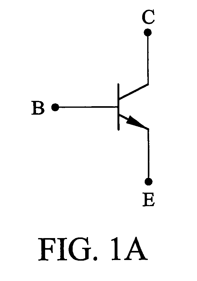
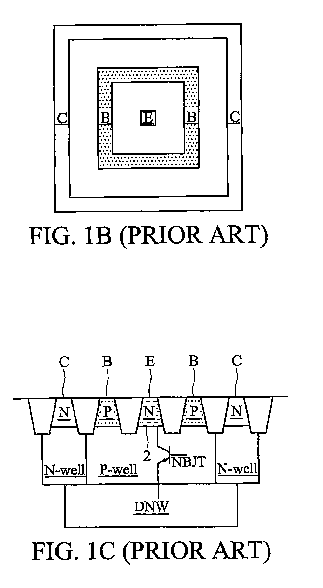
High-gain vertex lateral bipolar junction transistor
a lateral bipolar junction transistor, high-gain technology, applied in logic circuits, logic functions, pulse techniques, etc., can solve the problems of increasing the cost of greater parasitic bjt, reducing the effect of vertical bjt parasitic effects, and limiting the gain of conventional vertical bjts and lateral bjts, so as to reduce the parasitic effect of vertical bjts and improve the current gain , the effect of increasing the direct emitter-
- Summary
- Abstract
- Description
- Claims
- Application Information
AI Technical Summary
Benefits of technology
Problems solved by technology
Method used
Image

Examples
Embodiment Construction
[0022]The making and using of the presently preferred embodiments are discussed in detail below. It should be appreciated, however, that the present invention provides many applicable inventive concepts that can be embodied in a wide variety of specific contexts. The specific embodiments discussed are merely illustrative of specific ways to make and use the invention, and do not limit the scope of the invention.
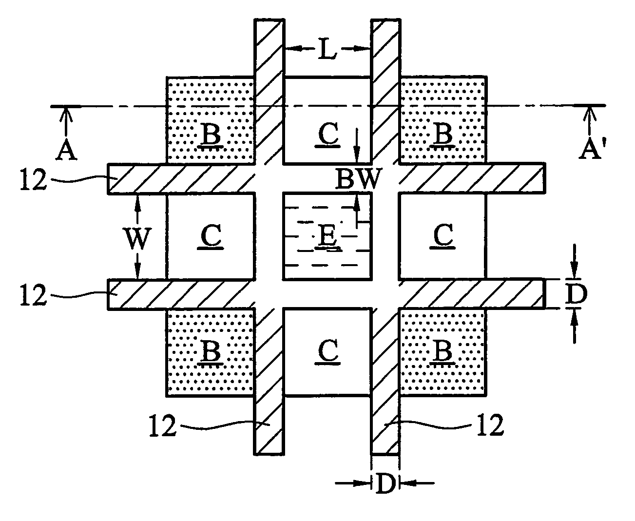
[0023]A novel design of lateral bipolar junction transistors (LBJT) with improved current gain is provided. The intermediate stages of manufacturing a preferred embodiment of the present invention are illustrated. The variations of the preferred embodiments are then discussed. Throughout the various views and illustrative embodiments of the present invention, like reference numbers are used to designate like elements.
[0024]In order to design a high current-gain LBJT, several principles are preferably applied. The base width, which is the distance in the base region separating...
PUM
| Property | Measurement | Unit |
|---|---|---|
| length | aaaaa | aaaaa |
| width | aaaaa | aaaaa |
| width | aaaaa | aaaaa |
Abstract
Description
Claims
Application Information