Check patentability & draft patents in minutes with Patsnap Eureka AI!

Methods of forming charge-trapping dielectric layers for semiconductor memory devices

a technology of dielectric layers and semiconductor memory, which is applied in the direction of semiconductor devices, electrical appliances, basic electric elements, etc., can solve the problems of data storage and other performance problems of memory devices, damage to the substrate/oxide layer interface, and non-volatile memory cells which employ charge-trapping layers and store charge in a localized manner. , to achieve the effect of reducing hydrogen concentration and hydrogen concentration

Active Publication Date: 2010-04-27
MACRONIX INT CO LTD
View PDF13 Cites 2 Cited by
  • Summary
  • Abstract
  • Description
  • Claims
  • Application Information

AI Technical Summary

Benefits of technology

This approach significantly reduces charge loss and improves data retention in semiconductor memory devices by minimizing hydrogen concentration at the oxide / substrate interface and repairing damage to the oxide layer, resulting in enhanced performance.

Problems solved by technology

Unfortunately, non-volatile memory cells which employ charge-trapping layers and store charge in a localized manner are not without problems.
The formation of bit lines in a substrate, for example, by ion implantation, can damage other layers of material (e.g., a silicon dioxide dielectric layer) which have already been deposited on the substrate and may also damage the substrate / oxide layer interface.
Such damage to these additional layers is believed to also cause data storage and other performance problems in memory devices.

Method used


Image

  • Methods of forming charge-trapping dielectric layers for semiconductor memory devices
  • Methods of forming charge-trapping dielectric layers for semiconductor memory devices
  • Methods of forming charge-trapping dielectric layers for semiconductor memory devices

Examples


Embodiment Construction

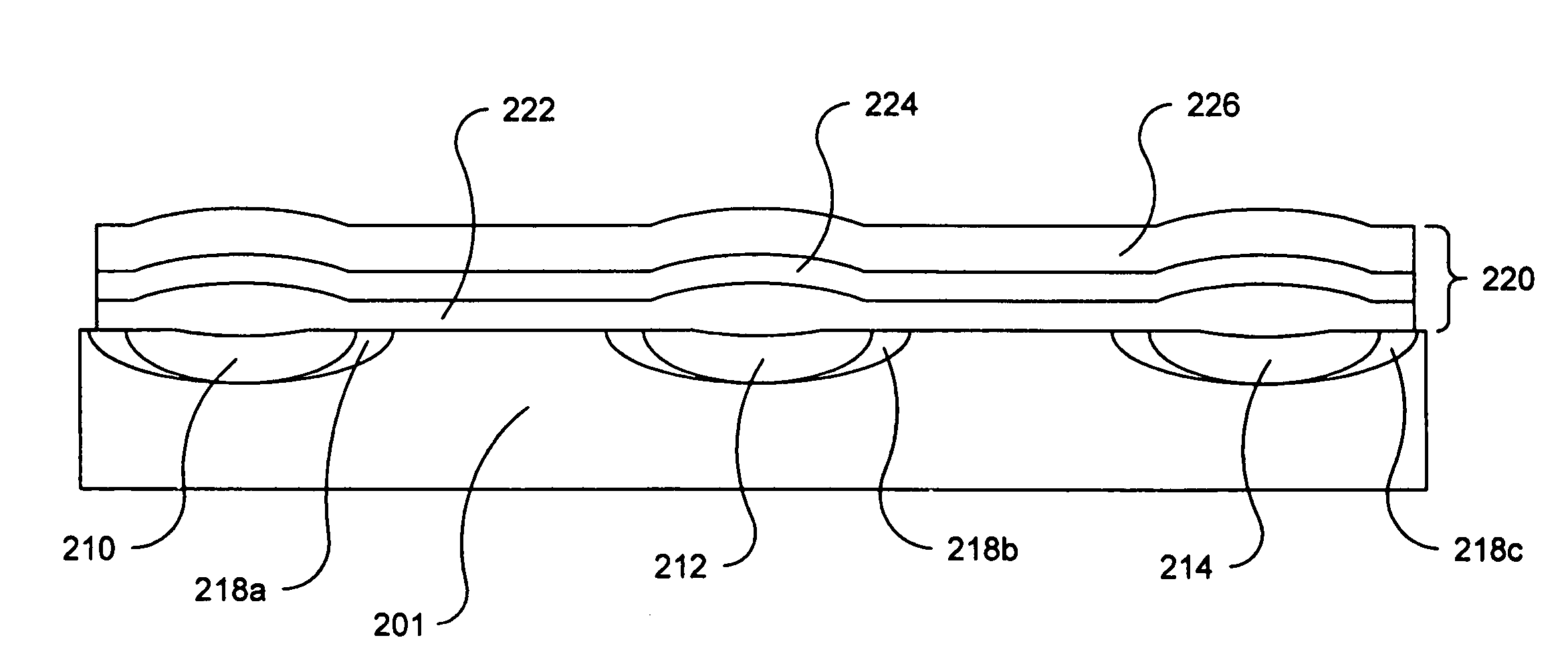
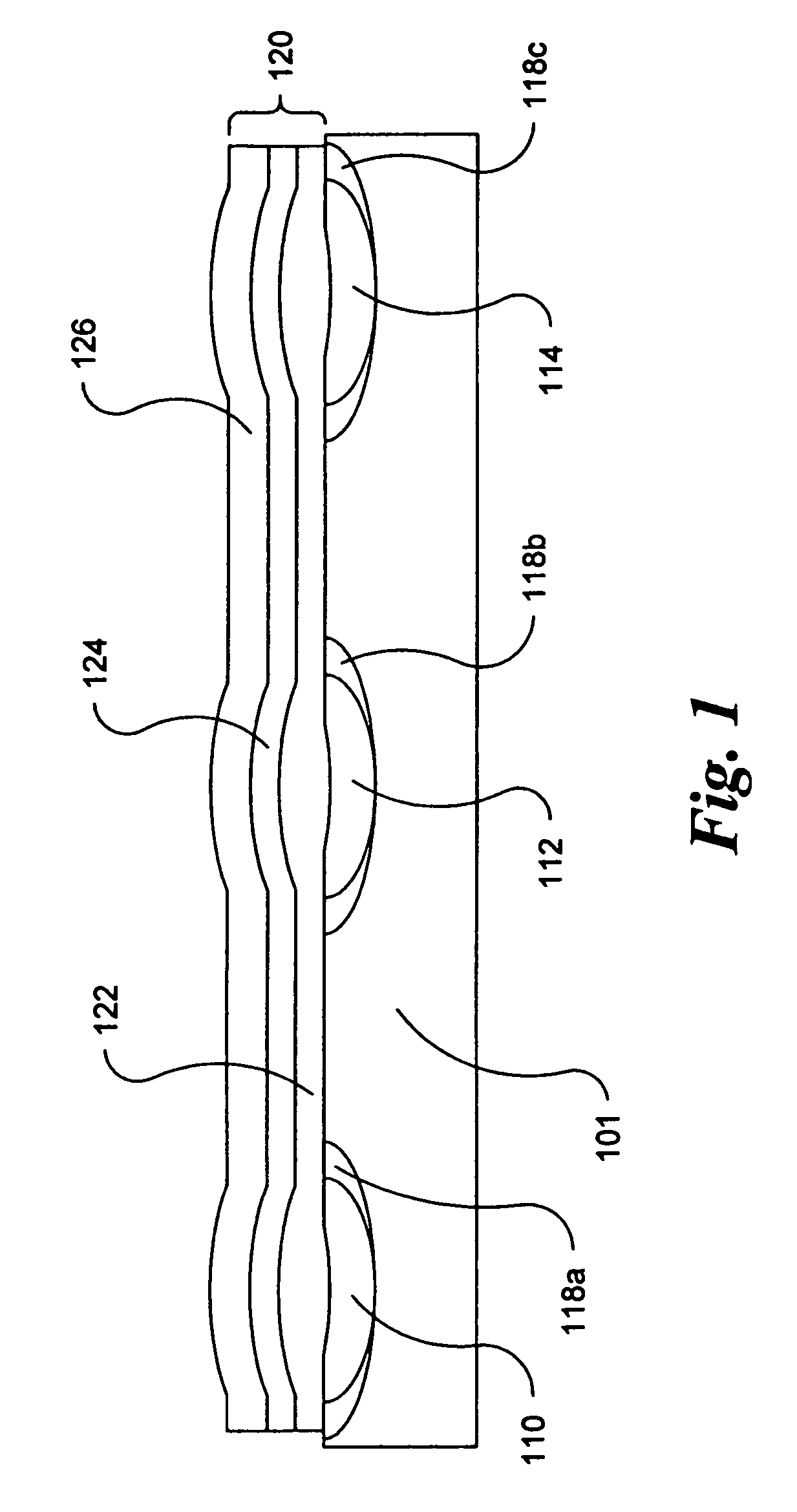
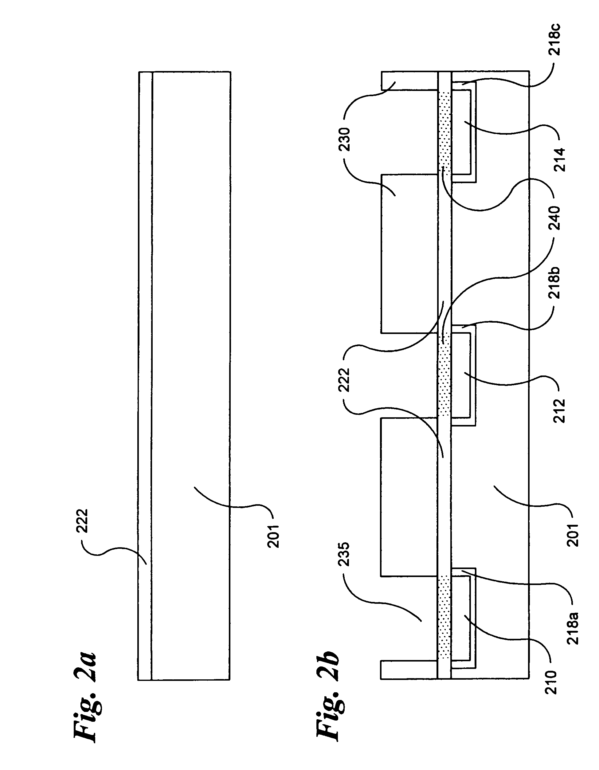
[0021]Reference will now be made in detail to the invention and the presently preferred embodiments thereof, examples of which are illustrated in the accompanying drawings. Wherever possible, the same or similar reference numbers are used in the drawings and the description to refer to the same or like parts. It should be noted that the drawings are in greatly simplified form and are not to precise scale. In reference to the disclosure herein, for purposes of convenience and clarity only, directional terms, such as top, bottom, left, right, up, down, above, below, beneath, rear, and front, are used with respect to the accompanying drawings. Such directional terms used in conjunction with the following description of the drawings should not be construed to limit the scope of the invention in any manner not explicitly set forth in the appended claims. Although the disclosure herein refers to certain illustrated embodiments, it is to be understood that these embodiments are presented b...


PUM

PropertyMeasurementUnit
temperatureaaaaaaaaaa
thicknessaaaaaaaaaa
thicknessaaaaaaaaaa

Abstract

Methods of forming charge-trapping dielectric layer structures in semiconductor memory devices which comprise: (a) providing a semiconductor substrate; (b) forming an oxide layer on at least a portion of the substrate; (c) forming two or more source / drain regions in the substrate below the oxide layer; (d) re-oxidizing the oxide layer; (e) forming a charge-trapping dielectric layer on the oxide layer; and (f) forming an insulating layer on the charge-trapping dielectric layer; as well as methods which comprise: (a) providing a semiconductor substrate; (b) forming an oxide layer on at least a portion of the substrate in a dry atmosphere; (c) forming two or more source / drain regions in the substrate below the oxide layer; (d) forming a charge-trapping dielectric layer on the oxide layer; (e) forming an insulating layer on the charge-trapping dielectric layer; and (f) annealing the insulating layer in an atmosphere having a hydrogen content of less than about 0.01% are described.

Description

BACKGROUND OF THE INVENTION[0001]Non-volatile memory (“NVM”) refers to semiconductor memory which is able to continually store information even when the supply of electricity is removed from the device containing the NVM cell. NVM includes Mask Read-Only Memory (Mask ROM), Programmable Read-Only Memory (PROM), Erasable Programmable Read-Only Memory (EPROM), Electrically Erasable Programmable Read-Only Memory (EEPROM), and Flash Memory. Non-volatile memory is extensively used in the semiconductor industry and is a class of memory developed to prevent loss of programmed data. Typically, non-volatile memory can be programmed, read and / or erased based on the device's end-use requirements, and the programmed data can be stored for a long period of time.[0002]Non-volatile memory cells generally include a charge-trapping layer structure situated between a control gate and a substrate having a source and a drain region. Often the charge-trapping structure is constructed of multiple layers, ...

Claims


Application Information

Patent Timeline
Patent Type & Authority Patents(United States)
IPC IPC(8): H01L21/425
CPCH01L21/2652H01L21/28211H01L27/115H01L27/11568H01L29/7923H01L21/28282H01L29/40117H10B69/00H10B43/30
Inventor SHIH, YEN-HAOLEE, SHIH-CHINHSIEH, JUNG-YULAI, ERH-KUNHSIEH, KUANG YEU
Owner MACRONIX INT CO LTD
Features
  • R&D
  • Intellectual Property
  • Life Sciences
  • Materials
  • Tech Scout
  • Unparalleled Data Quality
  • Higher Quality Content
  • 60% Fewer Hallucinations
Learn More