Memory device

a memory device and memory technology, applied in the field of memory devices, can solve the problems of large increase in the cost of fabrication equipment used to manufacture such miniaturised devices, physical phenomena that can have undesirable effects upon the operation of miniaturised conventional semiconductor devices, and the problem of reducing the efficiency of the miniaturisation of such steps, so as to achieve the effect of simple manufacturing, simple technique and memory uni

Active Publication Date: 2010-05-11
PRAGMATIC PRINTING
View PDF8 Cites 1 Cited by
  • Summary
  • Abstract
  • Description
  • Claims
  • Application Information

AI Technical Summary

Benefits of technology

[0008]The memory unit of such a device is relatively simple to manufacture, as the memory unit can utilise a single pattern of features to define the functionality of the unit. Thus, the device can be manufactured using a relatively simple technique compared with prior art processes of fabricating integrated circuits, which involve multiple steps involving overlying and aligning different shapes and patterns. Additionally, the memory unit is typically relatively small e.g. the unit can be of sub-micrometer dimensions, without deleteriously affecting the memory performance.

Problems solved by technology

However, miniaturisation of such steps (to manufacture devices of sub-micrometer dimensions e.g. nanometre dimensions) is problematic for a number of reasons, including the precise alignment of the apparatus required between each of the different steps.
This leads to a relatively large increase in cost of the fabrication equipment utilised to manufacture such miniaturised devices.
Additionally, as semiconductor device dimensions rapidly reduce to the nanometre scale, physical phenomena arise that can have undesirable effects upon the operation of the miniaturised conventional semiconductor devices.
A single charged impurity in the close vicinity of a SET can seriously influence its operation.
Thus, the performance of existing electronic devices can deteriorate, upon miniaturisation, unless a high degree of control of surface physical and chemical properties can be realised.

Method used


Image

  • Memory device
  • Memory device
  • Memory device

Examples


Embodiment Construction

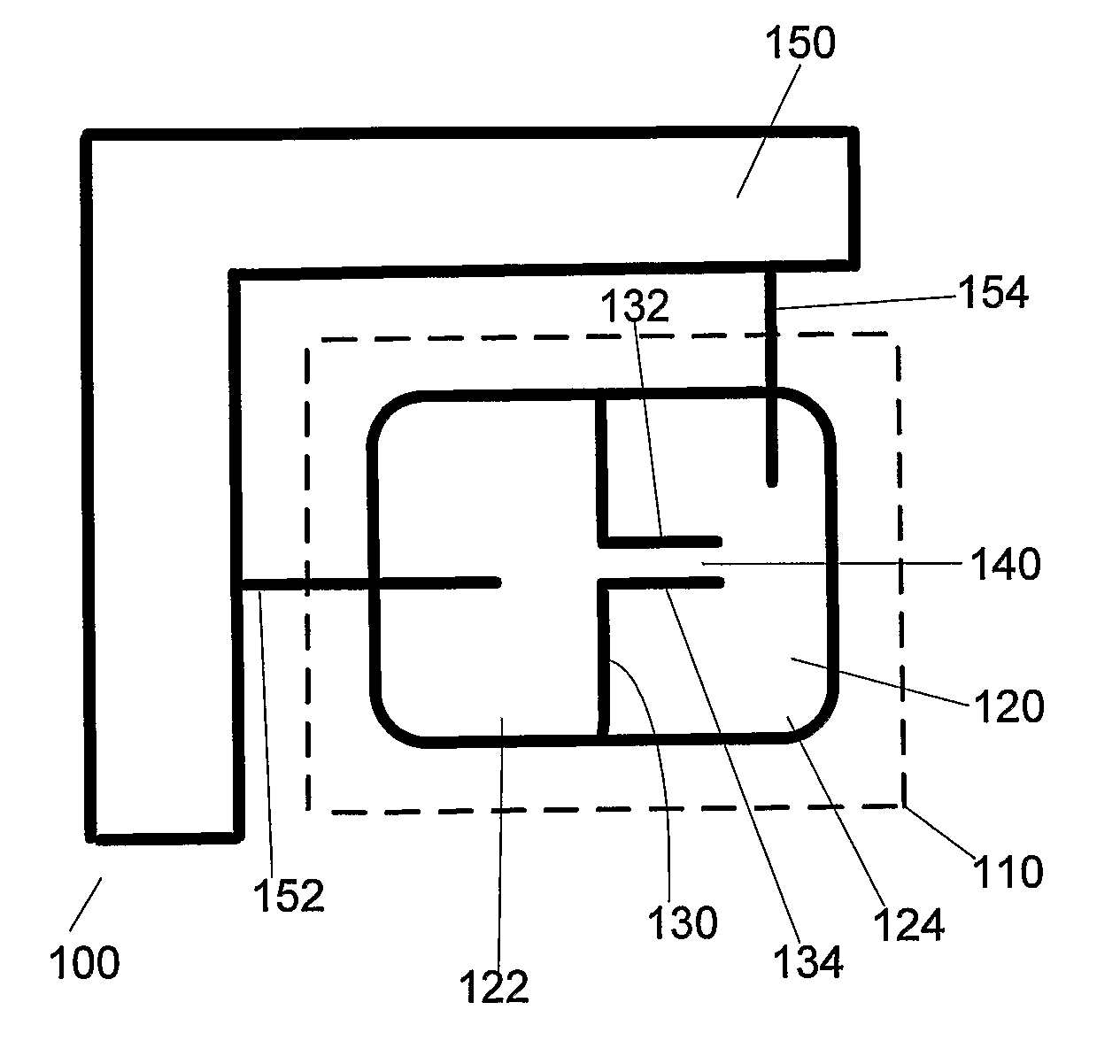
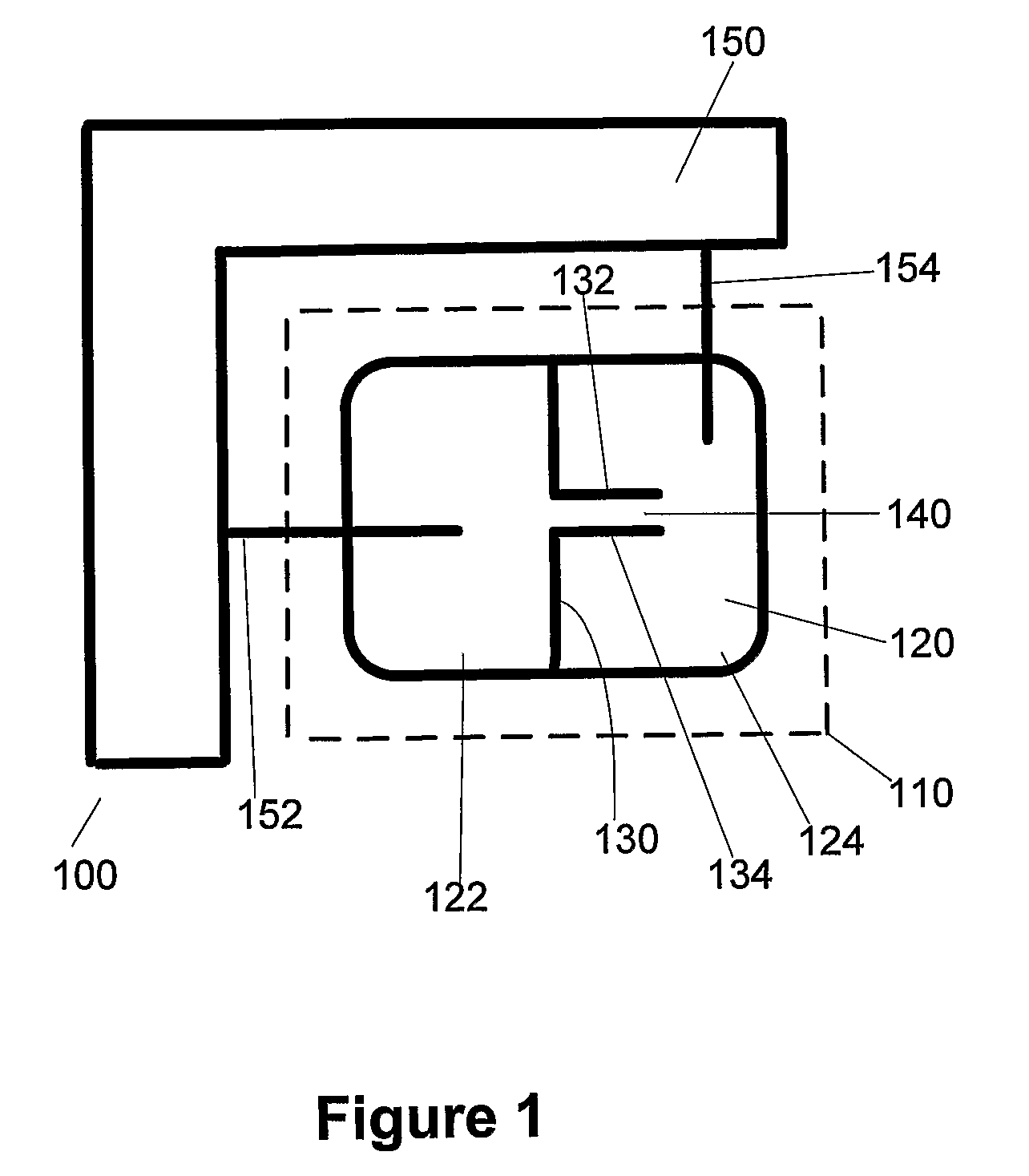
[0036]FIG. 1 shows a nanometre-scale memory device 100 in accordance with an embodiment of the present invention. The device 100 comprises a memory unit 110 comprising a substrate 120 supporting mobile charge carriers (e.g. electrons or holes). Insulative features 130, 132, 134 are formed on the substrate surface to define first and second substrate areas 122, 124 on either side of the insulative features 130, 132, 134. The insulative features 132, 134 define a channel 140 connecting the first substrate area 122 to the second substrate area 124. The elongate channel 140 provides a charge carrier flow path from the first area to the second area. The insulative features extend to the edges of the device surface.

[0037]The elongate channel 140 is dimensioned such that the parameters of the charge carrier flow path are dependent on the potential difference between the first and second areas 122, 124. A first electrode 152 is coupled to the first area 122 for providing a voltage to that a...


PUM

PropertyMeasurementUnit
distanceaaaaaaaaaa
lengthaaaaaaaaaa
threshold voltageaaaaaaaaaa

Abstract

A memory device includes a memory unit comprising a substrate supporting mobile charge carriers. Insulative features formed on the substrate surface define first and second substrate areas on either side of the insulative features areas being connected by an elongate channel defined by the insulative features. The memory unit is switchable between first and second states in which the channel respectively provides a first conductance and a second, different conductance between the first and second areas at a predetermined potential difference between said first and second. A write circuit is arranged to apply a first potential difference across the first and second areas for changing the memory unit to the first state, and a second, different potential difference for changing the memory unit to the second state. A read circuit is arranged to apply the predetermined potential difference across the first and second areas for reading the state.

Description

BACKGROUND OF THE INVENTION[0001]The present invention relates to a memory device, to methods and apparatus for writing to and reading from the memory, and to associated methods of manufacture. Particularly embodiments of the present invention are suitable for, but not limited to, use as a memory for a computer.[0002]A memory is a device used to store information for subsequent retrieval. The memory may be associated with a computer, or a device including a computational unit e.g. a mobile phone. Information is typically stored in digital form as sequences of bits.[0003]Memory devices can be permanently connected to computational devices, or can be separate devices (e.g. secure digital flash memory) arranged to be removably connected to computational devices. Memory devices are now incorporated within a range of media e.g. many banking cards now incorporate a memory device, for storage of the PIN (personal identification number) of the user, on the card.[0004]There is an ongoing des...

Claims


Application Information

Patent Timeline
Patent Type & Authority Patents(United States)
IPC IPC(8): G11C11/36G11C11/00
CPCB82Y10/00G11C11/00Y10T29/49002
Inventor SONG, AIMIN
Owner PRAGMATIC PRINTING
Why Eureka
Try Eureka