Method of processing resist, semiconductor device, and method of producing the same

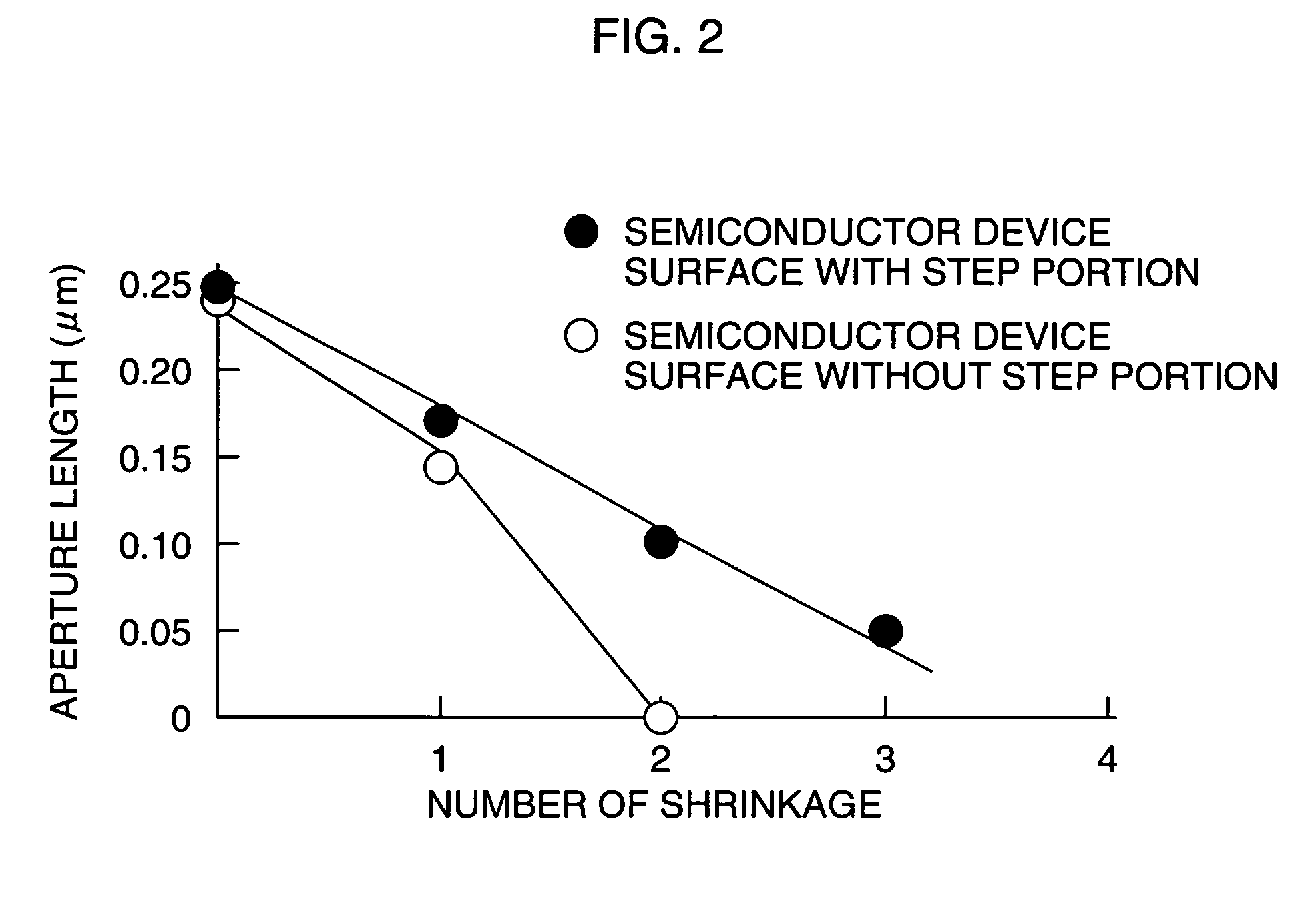
a technology of semiconductor devices and resists, which is applied in the direction of semiconductor devices, photosensitive material processing, electrical equipment, etc., can solve the problems of reducing the wavelength of light sources to form minute resist apertures, reducing the aperture length, and reducing the cost of equipment and masks. the effect of 0.05 m

Active Publication Date: 2010-05-18
FUJITSU LTD
View PDF17 Cites 33 Cited by
  • Summary
  • Abstract
  • Description
  • Claims
  • Application Information

AI Technical Summary

Problems solved by technology

However, decreasing the wavelength of the light source to form minute resist apertures is costly, because the equipment and masks are expensive.
Therefore there is a need for a technique to form a minute aperture by electron beam lithography equipment using an inexpensive light source or having a stable technical level, but the amount of reduction in the aperture length has been limited to 0.05 μm with conventional resist deformation (heat treatment, mixing) technology.

Method used


Image

  • Method of processing resist, semiconductor device, and method of producing the same
  • Method of processing resist, semiconductor device, and method of producing the same
  • Method of processing resist, semiconductor device, and method of producing the same

Examples


embodiment 1

[0047]In this embodiment, the present invention is applied in forming minute contact holes in an interlayer insulator film to manufacture transistors.

[0048]FIGS. 3A to 3C and FIGS. 4A to 4C are schematic sectional views showing the method of manufacturing a transistor in order of steps according to embodiment 1.

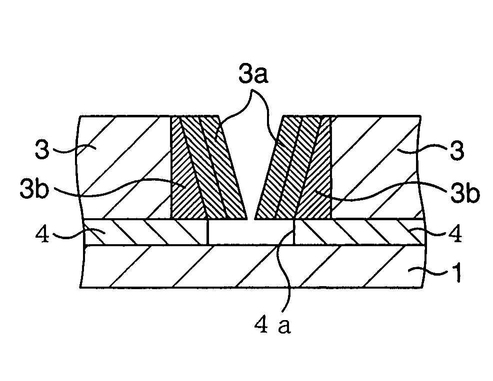
[0049]As shown in FIG. 3A, a gate electrode 12 and a source / drain 13 which is a pair of ohmic electrodes are formed on a semiconductor substrate 11.

[0050]Then polyimide resin is applied to a coating thickness of about 1.0 μm by the spin coat method so as to cover the gate electrode 12 and the source / drain 13, and heat treated to form an interlayer insulator film 14. The interlayer insulator film 14 may be a single-layer film consisting of only polyimide resin or a multilayer film consisting of two or more different materials, such as a film consisting of polyimide resin and a nitride film deposited thereon. A resist (for example, PFI-32A, Sumitomo Chemical Co., Ltd.) is appli...

embodiment 2

[0060]In this embodiment, the present invention is applied in forming what is generally called mushroom type gate electrodes using electron beam lithography to manufacture transistors.

[0061]FIGS. 5A to 5D and FIGS. 6A to 6D are schematic sectional views showing the method of manufacturing a transistor in order of steps according to embodiment 2.

[0062]As shown in FIG. 5A, a buffer layer, an InGaAs channel layer, an AlGaAs electron-supplying layer and a GaAs low-resistance layer are first grown sequentially on a semi-insulating GaAs substrate by the MOCVD method to form a compound semiconductor substrate 21, and an active region is formed by oxygen impregnation to form, for example, the source / drain 22, which is a pair of ohmic electrodes consisting of AuGe / Au with a coating thickness of about 20 nm / 200 nm.

[0063]The low-resistance layers about 0.1 μm wide at both ends of the gate finger in the active region are removed by etching to form a groove 42, and a surface component film 23 co...

modified embodiment

[0077]This is another aspect of embodiment 2. In this embodiment, the present invention is applied in forming what is generally called mushroom type gate electrodes using electron beam lithography to manufacture transistors.

[0078]FIGS. 7A to 7D and FIGS. 8A to 8D are schematic sectional views showing the method of manufacturing a transistor in order of steps according to modified embodiment 2.

[0079]As shown in FIG. 7A, a buffer layer, an InGaAs channel layer, an AlGaAs electron-supplying layer and a GaAs low-resistance layer are first grown sequentially on a semi-insulating GaAs substrate by the MOCVD method to form a compound semiconductor substrate 21, and an active region is formed by oxygen impregnation to form, for example, the source / drain 22, which is a pair of ohmic electrodes consisting of AuGe / Au with a coating thickness of about 20 nm / 200 nm.

[0080]A surface component film 23 consisting of, for example, silicon nitride is formed on the compound semiconductor substrate 21 s...


PUM

PropertyMeasurementUnit
aperture lengthaaaaaaaaaa
wavelengthaaaaaaaaaa

Abstract

A surface component film (2) is etched using a resist (3) as a mask, and the surface component film (2) is patterned according to the shape of an aperture (3a). This results in a step portion (4) having the same shape as the aperture (3a), with the sidewall (4a) of the step portion (4) exposed through the aperture (3a). The aperture (3a) is spin-coated with a shrink agent, reacted at a first temperature, and developed to shrink the aperture (3a). To control the shrinkage with high accuracy, in the first round of reaction, the aperture is shrunk by, for example, about half of the desired shrinkage. The aperture (3a) is further spin-coated with a shrink agent, reacted at a second temperature, and developed to shrink the aperture (3a). In this embodiment, the second-round shrink process will result in the desired aperture length. The second temperature is adjusted based on the shrinkage in the first round. With respect to a resist using short-wavelength light (short-wavelength resist) or a resist using electron beam (electron beam resist), a minute aperture can be obtained with stable shrink effect and accurate control of the length thereof.

Description

[0001]This application is a continuation of international application PCT / JP03 / 05828 filed May 9, 2003.TECHNICAL FIELD[0002]The present invention relates to a method of processing a resist, a semiconductor device and a method of producing the same, and is directed to a technology to shrink a resist aperture stably and dramatically to achieve fine patterns.BACKGROUND ART[0003]In recent years, minimization technology has been used extensively for wiring and so forth to meet the need for reduction in the circuit area and increase in the performance of semiconductor memories and system LSI devices, and latest lithographic techniques will be presently used, in particular, for the microfabrication of contact holes connecting wiring layers. On the other hand, transistors with superior high-frequency characteristics require minute gate electrodes, and transistors having minute gate electrodes, and especially compound semiconductors, are useful for signal processing (optical communication) a...

Claims


Application Information

Patent Timeline
Patent Type & Authority Patents(United States)
IPC IPC(8): H01L21/027H01L21/469G03F7/40H01L21/28H01L21/768
CPCG03F7/40H01L21/0273H01L21/28114H01L21/76802H01L2924/0002H01L2924/00
Inventor MAKIYAMA, KOZOSAWADA, KEN
Owner FUJITSU LTD
Why Eureka
Try Eureka