Image sensor for detecting wide spectrum and method of manufacturing the same

a wide spectrum, image sensor technology, applied in the field of image sensors, can solve the problems of increased cost, mechanical/thermal/optical distortion, etc., and achieve the effect of enhancing photoelectric conversion efficiency and reducing light loss

Active Publication Date: 2010-05-25
HANVISION +1
View PDF3 Cites 53 Cited by
  • Summary
  • Abstract
  • Description
  • Claims
  • Application Information

AI Technical Summary

Benefits of technology

[0012]The present invention provides an image sensor for detecting a wide spectrum, in which a plurality of light receiving layers, each light receiving layer absorbing light with an individual wavelength range, are stacked on a semiconductor device. Also, the present invention provides a semiconductor device to detect spectrums of various rays, such as ultraviolet rays, visible rays, near-infrared rays, far-infrared rays, and middle infrared rays, individually, according to their wavelengths, in a single pixel, thereby reducing light losses and enhancing photoelectric conversion efficiency.

Problems solved by technology

However, in the case where two or more image sensors or cameras are used, a serious problem occurs in an optical arrangement upon manufacturing the image sensors or cameras, and mechanical / thermal / optical distortion is generated due to environmental factors.
Accordingly, an electrical / mechanical / optical system for compensating for such mechanical / thermal / optical distortion is needed, which results in an increase of cost.

Method used


Image

  • Image sensor for detecting wide spectrum and method of manufacturing the same
  • Image sensor for detecting wide spectrum and method of manufacturing the same
  • Image sensor for detecting wide spectrum and method of manufacturing the same

Examples


Embodiment Construction

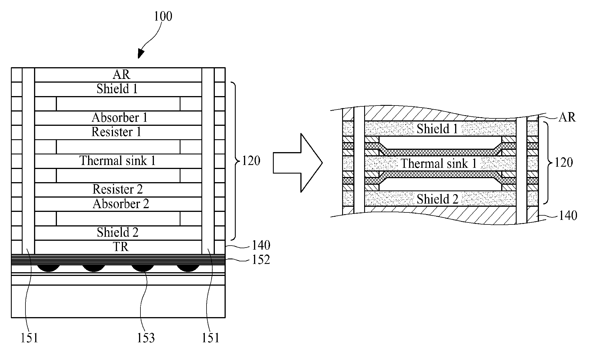
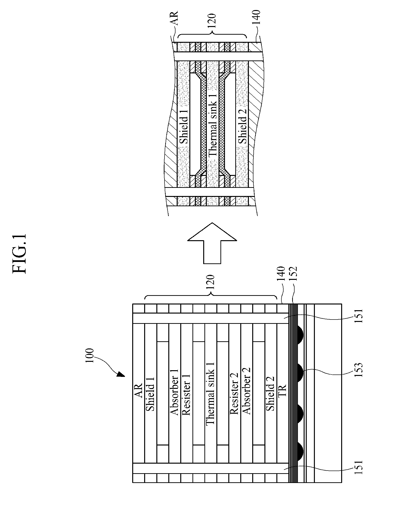
[0037]The invention is described more fully hereinafter with reference to the accompanying drawings, in which exemplary embodiments of the invention are shown. This invention may, however, be embodied in many different forms and should not be construed as limited to the exemplary embodiments set forth herein. Rather, these exemplary embodiments are provided so that this disclosure is thorough, and will fully convey the scope of the invention to those skilled in the art. In the drawings, the size and relative sizes of layers and regions may be exaggerated for clarity. Like reference numerals in the drawings denote like elements.

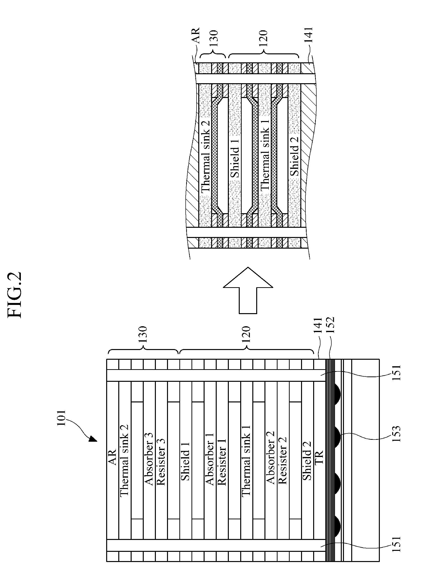
[0038]FIG. 1 is a sectional view of an image sensor 100 for detecting a wide spectrum, according to an exemplary embodiment, and FIG. 2 is a sectional view of an image sensor 101 for detecting a wide spectrum, according to another exemplary embodiment. The right sides of FIGS. 1 and 2 show the sectional views of portions of the image sensors 100 and 101 when t...


PUM


Abstract

An image sensor for detecting a wide spectrum includes a plurality of infrared ray receiving layers which individually receive infrared rays having different wavelengths for each pixel, the plurality of infrared ray receiving layers stacked to each other. The image sensor, which is an integrated image sensor where at least two micro bolometers are stacked, acquires spectrum information about visible rays and near-infrared rays as well as two or more infrared rays applied on an object, without mechanical / thermal / optical distortion, and provides the spectrum information to a silicon-based semiconductor such as a photodiode, thereby improving photoelectric conversion efficiency.

Description

BACKGROUND OF THE INVENTION[0001]1. Field of the Invention[0002]The present invention relates to an image sensor, and more particularly, to an image sensor for detecting a wide spectrum, in order to effectively detect various visible and infrared spectrum and accordingly enhance photoelectric conversion efficiency.[0003]2. Description of the Related Art[0004]In general, an image sensor is an electrical device for converting an optical image, that is, changes in light, into an electrical signal, and is used widely in mobile phones, digital still cameras, personal digital assistants (PDAs), toys, electronic games, robots, personal computer cameras, optical computer mice, office scanners, security surveillance cameras, night infrared cameras, recognition systems, biometric systems, wireless endoscopes, etc.[0005]Meanwhile, one of various methods for obtaining visible images is to obtain visible color images in a visible region having wavelengths of 400 through 700 nm using a TV camera,...

Claims


Application Information

Patent Timeline
Patent Type & Authority Patents(United States)
IPC IPC(8): G01J5/00
CPCG01J3/36G01J5/04G01J5/045G01J5/06H04N5/332H01L27/14652G01J5/20H01L27/14647H04N5/33H04N23/11
Inventor HANNEBAUER, ROBERT
Owner HANVISION
Why Eureka
Try Eureka