Method for effective refractive index trimming of optical waveguiding structures and optical waveguiding structures

a technology of optical waveguides and trimming methods, applied in the field of effective refractive index trimming of optical waveguides and optical waveguides, can solve the problems of ring resonators being highly sensitive to fabrication errors, affecting the behavior or the properties of optical components, and unattractive for mass fabrication, so as to increase the effective refractive index, and reduce the effect of ring resonators

Inactive Publication Date: 2010-05-25
INTERUNIVERSITAIR MICRO ELECTRONICS CENT (IMEC VZW) +1
View PDF9 Cites 1 Cited by
  • Summary
  • Abstract
  • Description
  • Claims
  • Application Information

AI Technical Summary

Benefits of technology

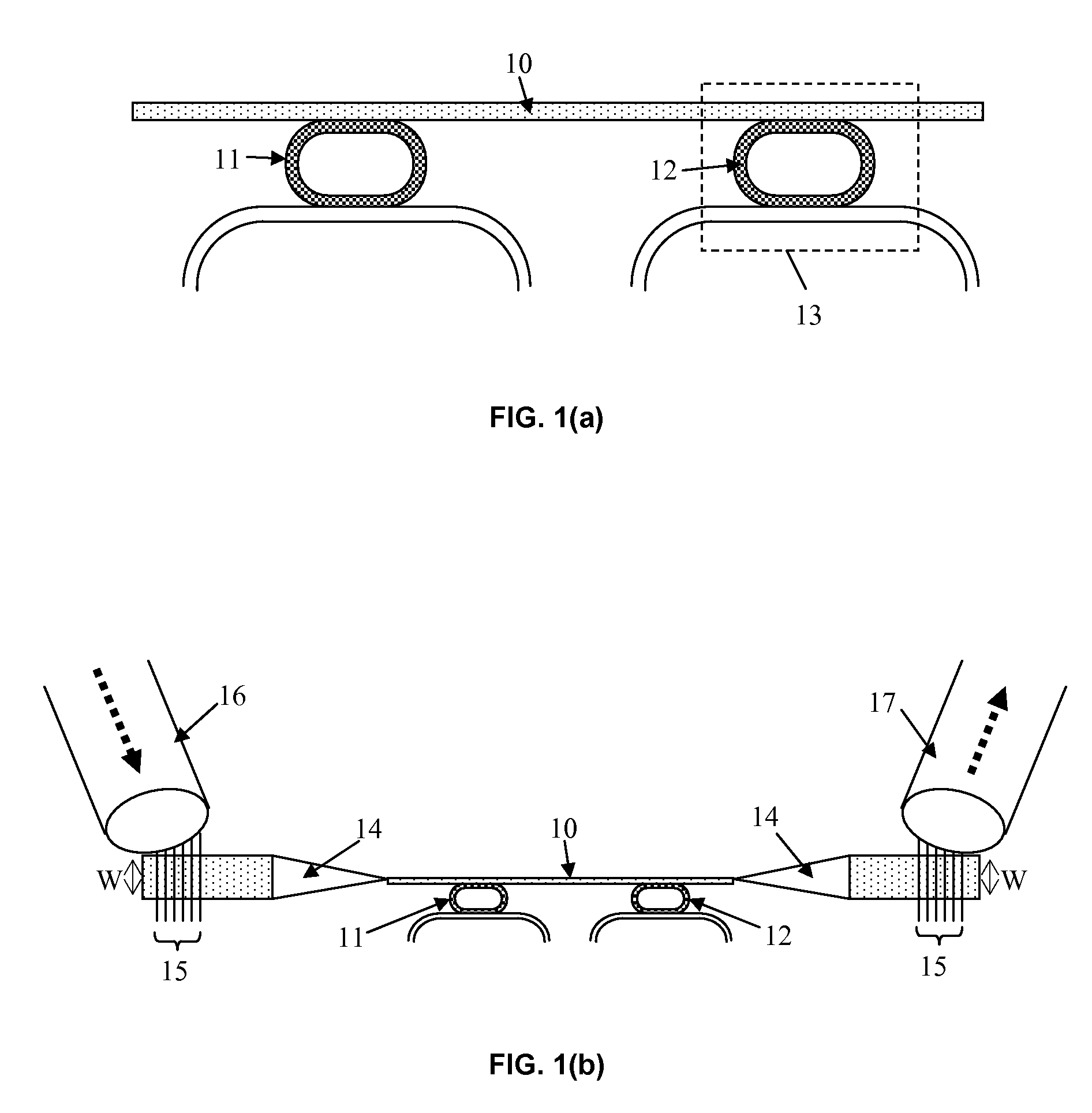
[0014]The present disclosure is particularly useful for effective refractive index trimming of optical waveguiding structures formed in a material system wherein the light guiding layer or core layer is not susceptible to compaction by irradiation, such as for example compaction by UV irradiation or by electron beam irradiation, although the disclosure is not restricted thereto and can also be applied to systems wherein the core material is a compactible material. The method of the present disclosure can for example be used for post-fabrication trimming of an effective refractive index of optical waveguiding structures formed in a material system with a large difference in refractive index (e.g. difference in refractive index>1) between a core material and a cladding material, for example a material system comprising a cladding material such as SiO2, SiN, SiON, Al2O3, TiO2, spin-on glass or borophosphosilicate glass and a core material such as silicon, InP, GaAs or ZnS, such as e.g. a silicon / oxide material system. The method allows local and independent trimming of an operating wavelength, e.g. resonance wavelength, of optical components on a chip and it allows compensating for operating wavelength variations, e.g. resonance wavelength variations.
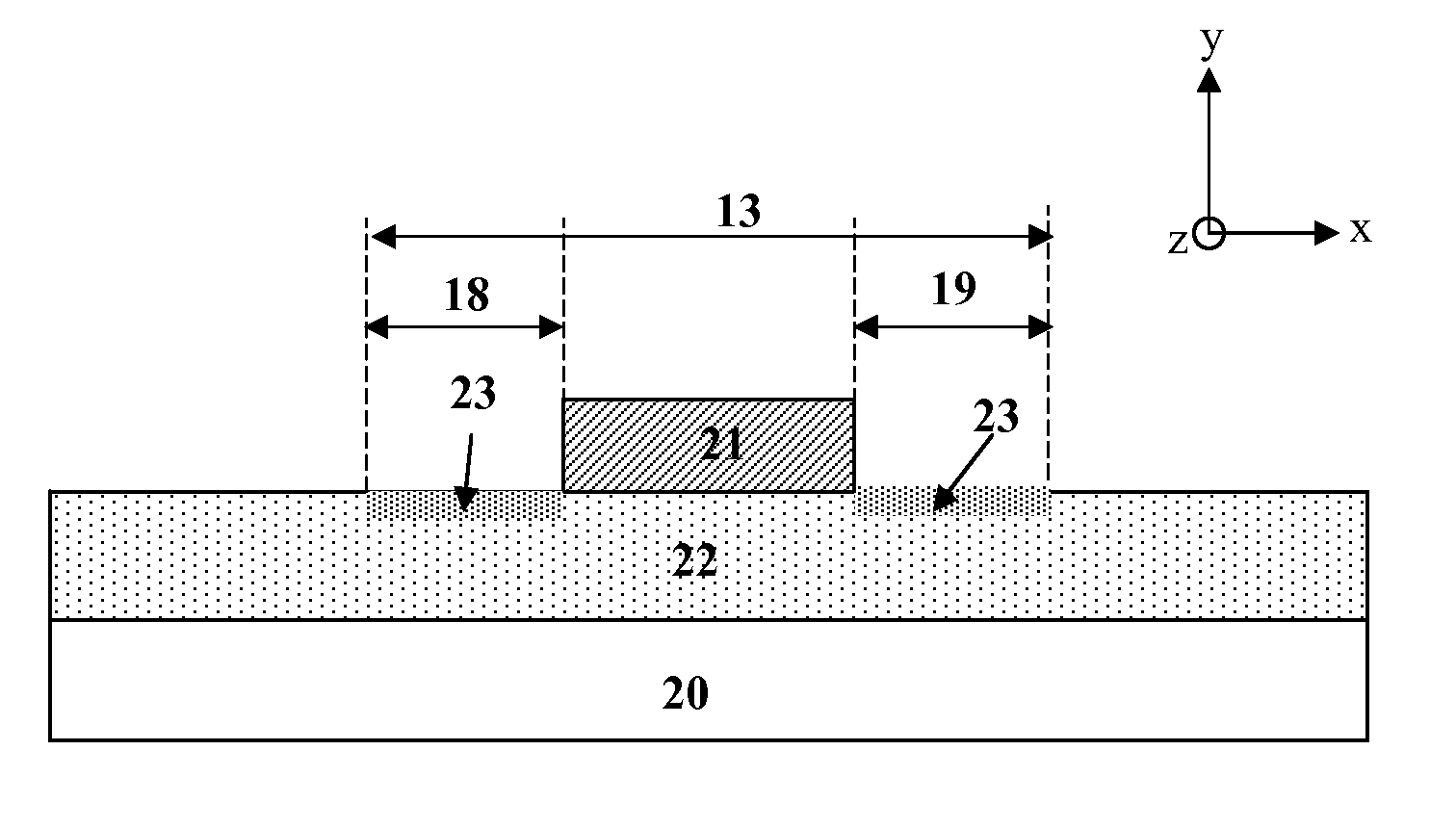
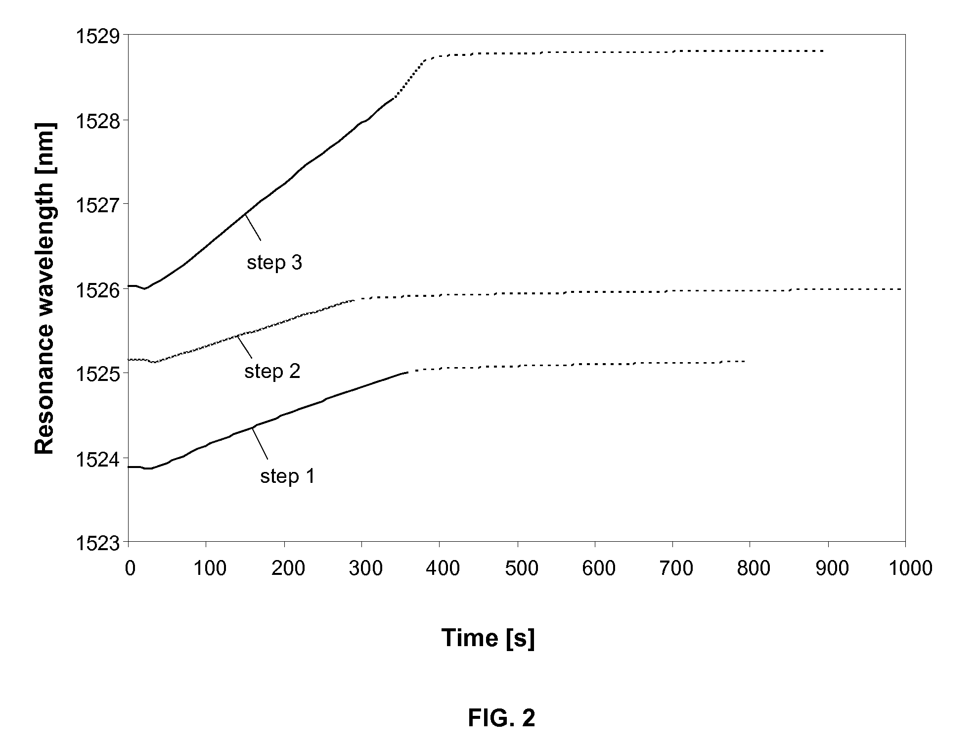
[0015]According to the disclosure, it has been found that by compaction of the cladding material in a compaction area next to patterns or ridges that are formed in the core material for realizing an optical waveguiding structure, the effective index of refraction of the optical waveguiding structure can be trimmed and thus the operating wavelength of an optical component comprising such an optical waveguiding structure can be trimmed. Compaction of the cladding material can for example be done by means of electron beam irradiation, ion beam irradiation or by UV irradiation. Due to the limited light confinement in the cladding layer, the trimming range for e.g. the resonance wavelength of an optical component such as a ring resonator is expected to be very limited (<1 nm). However, it was surprisingly found that the trimming range can be greatly increased (>5 nm) by compacting the cladding material next to (so not underneath) and at both sides of the patterns or ridges defined in the core material for forming optical components. In this context, the cladding material next to the ridges refers to a volume of the cladding material that, after orthogonal projection of the structure on a plane parallel to the cladding surface, would be adjacent to (i.e. touching or near or close to) and not overlapping the ridges. By appropriate selection of the irradiation energy, i.e. using an irradiation energy that is sufficiently low for preventing penetration of the radiation through the core layer, the volume compaction can be restricted to the cladding material next to the ridges of core material. In other embodiments the volume compaction can be restricted to the cladding material next to the ridges by shielding the ridges from the irradiation. It has been found that compaction of the cladding material next to the ridges, at both sides of the ridges, causes tensile strain in the core material. The tensile strain results in a change in the refractive index of the core material, e.g. an increase in the refractive index in case the core material is silicon. In this case the effect of the cladding material compaction on the effective refractive index is thus strengthened by the strain it induces in the silicon core. Both effects can generate an increase in effective refractive index, which may for example result in a red shift of an operating wavelength, e.g. resonance wavelength, of an optical component.

Problems solved by technology

This can for example be done with electron beam lithography, which is however a serial fabrication technique and therefore unattractive for mass fabrication.
These variations can be caused by wafer non-uniformity or by non-uniformity within one chip and can affect the behavior or the properties of the optical component.
For example, ring resonators are highly sensitive to fabrication errors.
A fabrication error of 1 nm typically leads to a 1 nm shift of the resonance wavelength.
In practice the resonance wavelength shift can exceed 1 nm, which is unacceptable for many applications.
Even the fabrication of identical devices on one wafer is difficult due to wafer scale variations.
However, if one envisages a plurality of components, e.g. resonators, on a single chip, thermal tuning with electrical heaters requires the incorporation of a heater for every resonator, which may lead to high power consumption and a high device complexity.

Method used


Image

  • Method for effective refractive index trimming of optical waveguiding structures and optical waveguiding structures
  • Method for effective refractive index trimming of optical waveguiding structures and optical waveguiding structures
  • Method for effective refractive index trimming of optical waveguiding structures and optical waveguiding structures

Examples


Embodiment Construction

[0032]In the following detailed description, numerous specific details are set forth in order to provide a thorough understanding of the disclosure and how it may be practiced in particular embodiments. However it will be understood that the present embodiments may be practiced without these specific details. In other instances, well-known methods, procedures and techniques have not been described in detail, so as not to obscure the present embodiments. While the present disclosure will be described with respect to particular embodiments and with reference to certain drawings, the reference is not limited hereto. The drawings included and described herein are schematic and are not limiting. It is also noted that in the drawings, the size of some elements may be exaggerated and, therefore, not drawn to scale for illustrative purposes.

[0033]Furthermore, the terms first, second and the like in the description, are used for distinguishing between similar elements and not necessarily for...


PUM


Abstract

A method for trimming an effective refractive index of optical waveguiding structures made for example in a high refractive index contrast material system. By compaction of cladding material in a compaction area next to patterns or ridges that are formed in the core material for realizing an optical waveguiding structure, the effective index of refraction of the optical waveguiding structure can be trimmed. Thus, the operating wavelength of an optical component comprising such an optical waveguiding structure can be trimmed. An optical waveguide structure thus obtained is also disclosed.

Description

CROSS-REFERENCE TO RELATED APPLICATIONS[0001]This application claims priority to U.S. Provisional Application Ser. No. 61 / 021,250 filed Jan. 15, 2008, the contents of which are incorporated by reference herein in its entirety.TECHNICAL FIELD[0002]This disclosure relates to a method for trimming an effective refractive index of optical waveguiding structures made for example in a high refractive index contrast material system, for example an SOI material system, and to optical waveguiding structures thus obtained.BACKGROUND[0003]Silicon-on-insulator (SOI) is gaining interest as a material system for ultra-compact integrated photonic circuits. An advantage of this material system is the high refractive index contrast between the silicon and the adjacent oxide or air, enabling small bend radii and dense integration. Furthermore, as silicon is the standard material that is used for microelectronic integrated circuits, this opens the door for photonics to use the standard, mature and com...

Claims


Application Information

Patent Timeline
Patent Type & Authority Patents(United States)
IPC IPC(8): G02B6/10G02B6/00
CPCB82Y20/00G02B6/1223G02B2006/12061G02B2006/12097G02B2006/12166
Inventor SCHRAUWEN, JONATHANVAN THOURHOUT, DRIESBAETS, ROELAND
Owner INTERUNIVERSITAIR MICRO ELECTRONICS CENT (IMEC VZW)
Why Eureka
Try Eureka