Method, storage media storing program, and component for avoiding increase in delay time in semiconductor circuit having plural wiring layers

a semiconductor circuit and wiring layer technology, applied in the direction of semiconductor/solid-state device details, pulse techniques, instruments, etc., can solve the problems of delay circuit operation and multi-layer operation, and achieve the effect of avoiding an increase in delay tim

Inactive Publication Date: 2010-05-25
SOCIONEXT INC
View PDF41 Cites 6 Cited by
  • Summary
  • Abstract
  • Description
  • Claims
  • Application Information

AI Technical Summary

Benefits of technology

[0010]The challenge of the present invention is to provide a terminal layer setting method, and the related program, which is capable of setting up a wiring layer (i.e., terminal layer) at an extended destination of a cell or macro for the cell or macro mounted onto a board while avoiding an increase in a delay time.
[0012]Here, a judgment is given as to whether a wiring connecting the subject cell or macro with the cell or macro at the connecting destination is “longer” or “shorter” by comparing between a driving capacity of a subject cell or macro and a resistance of wiring for connecting the subject cell or macro with a cell or macro at the connecting destination. Accordingly, a setup of a wiring layer (i.e., terminal layer) at an extending destination of a wiring terminal of the subject cell or macro based on the comparison (i.e., judgment) result makes it possible to establish a wiring resistance at a reasonable level and set up a wiring layer (i.e., terminal layer) at the extending destination of the subject cell or macro while avoiding an increase in a delay time.
[0014]The normal direction to the surface which the subject cell or macro is mounted onto becomes the shortest path for the wiring terminal of the subject cell or macro extending to the wiring layer at the extended destination and therefore the above described delay time can be further suppressed.
[0016]According to the present invention, a judgment is given as to whether a wiring connecting the subject cell or macro with the cell or macro at the connecting destination is “longer” or “shorter” by comparing between the driving capacity of a subject cell or macro and the resistance of wiring for connecting the subject cell or macro with a cell or macro at the connecting destination. And accordingly, a setup of a wiring layer (i.e., terminal layer) at an extending destination of a wiring terminal of the subject cell or macro based on the comparison (i.e., judgment) result makes it possible to establish a wiring resistance at a reasonable level and set up a wiring layer (i.e., terminal layer) at the extending destination of the subject cell or macro while avoiding an increase in a delay time.

Problems solved by technology

With regard to a semiconductor circuit having such a plurality of layers, the problem is which of the plurality of layers to go through when connecting a cell or macro with the cell or macro for the respective mating connections as noted in a patent document 1 below for instance.
Such practices have created a lot of circuit wiring, also in lower circuit layers, that is, in a local layer with a large resistance, and using of a lot of Vias (also called “contact hole”), and thus caused delayed circuit operation.

Method used


Image

  • Method, storage media storing program, and component for avoiding increase in delay time in semiconductor circuit having plural wiring layers
  • Method, storage media storing program, and component for avoiding increase in delay time in semiconductor circuit having plural wiring layers
  • Method, storage media storing program, and component for avoiding increase in delay time in semiconductor circuit having plural wiring layers

Examples


Embodiment Construction

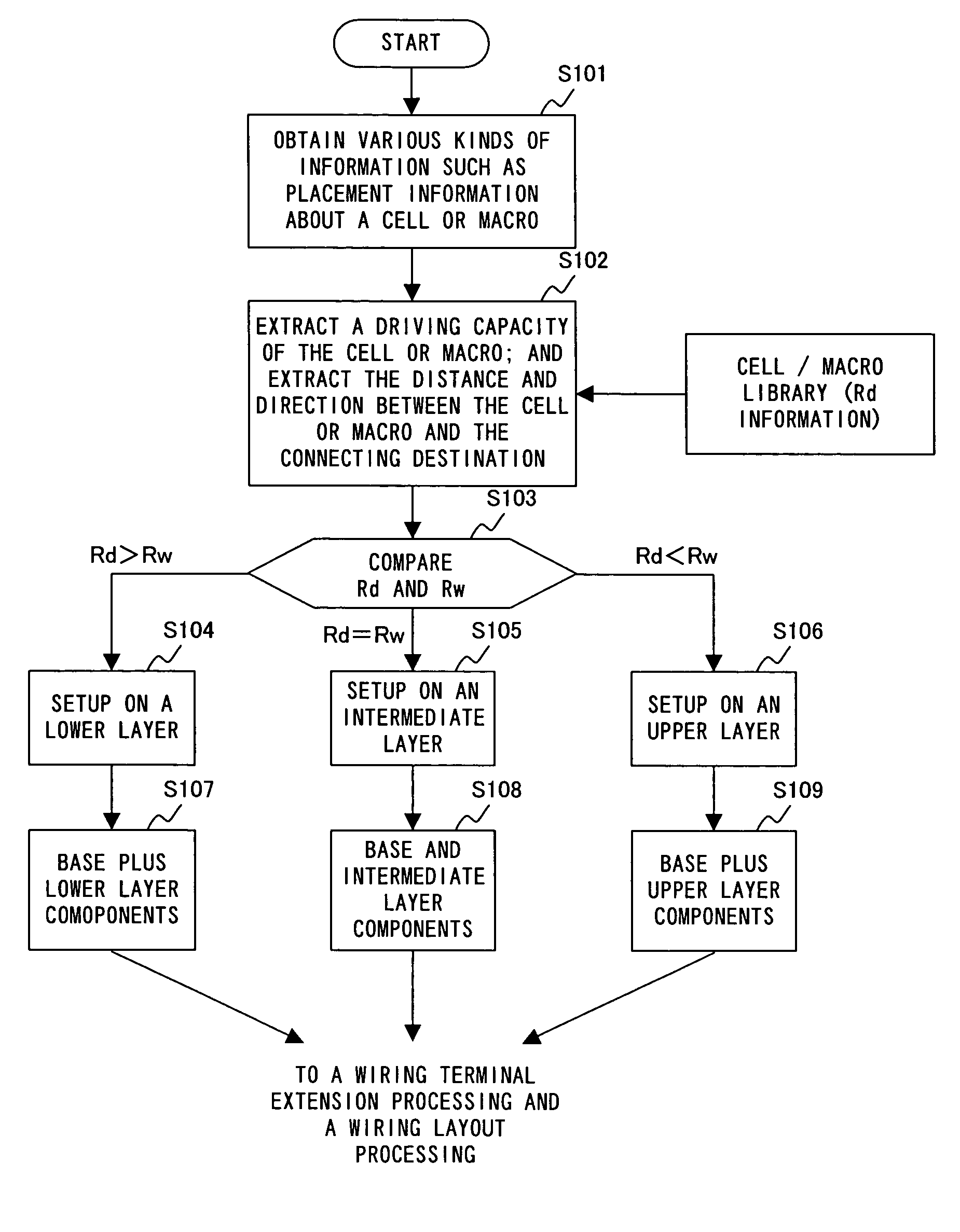
[0033]The following describes a preferred embodiment of the present invention in detail while referring to the accompanying drawings.

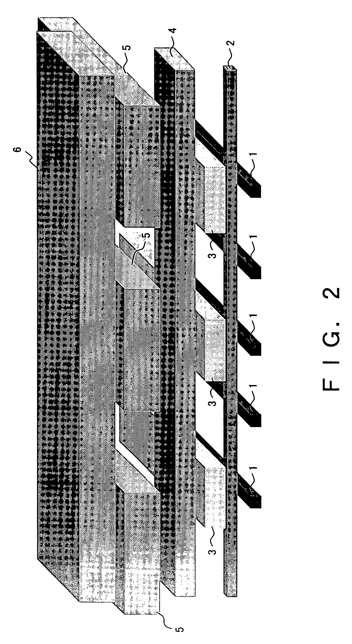
[0034]FIG. 2 is a oblique perspective view of a structure of a plurality of wiring layers comprised by a semiconductor circuit which a terminal layer setting processing according to a preferred embodiment of the present invention is applied to.

[0035]In FIG. 2, shows six wiring layers 1 through 6 set up on a board (not shown herein) which a cell or macro is mounted onto. Here, the wiring layers 1 and 2 are called local layers on which a wire width, a wire height and the pitch between wires are all the smallest among the wiring layers 1 through 6. The wiring layers 5 and 6 are called global layers in which a wire width, a wire height and the pitch between wires are all the largest among the wiring layers 1 through 6. The wiring layers 3 and 4 are called semi-global layers in which a wire width, a wire height and the pitch between wires are all in interme...


PUM


Abstract

A method for a computer setting up a terminal layer of a semiconductor circuit having plural wiring layers including obtaining various kinds of information such as placement information relating to a plurality of cells or macros of the semiconductor circuit and being mounted onto a circuit board from a storage unit of the computer; comparing a driving capacity of a subject cell or macro, which is contained in the obtained information, and a resistance of wiring for connecting the subject cell or macro with the cell or macro at a connecting destination; and setting up a terminal layer based on a result of the comparing.

Description

CROSS-REFERENCE TO RELATED APPLICATIONS[0001]This application is based upon and claims the benefit of priority from the prior Japanese Patent Application No. 2005-096133 filed on Mar. 29, 2005, the entire contents of which are incorporated herein by reference.BACKGROUND OF THE INVENTION[0002]1. Field of the Invention[0003]The present invention relates to a terminal layer setting method for a semiconductor circuit having a plurality of circuit layers, storage media storing a terminal layer setting program, storage media storing a circuit terminal extension processing program and a terminal extending component used for setting of the terminal layer.[0004]2. Description of the Related Art[0005]In recent years, with a quantum leap increase in the number of cells (e.g., logic gate, inverter and NAND) or macros (e.g., SRAM) which are equipped onto a board, separate layers for wiring between these cells and macros have evolved to a plurality of layers, parallel with, and independent of, th...

Claims


Application Information

Patent Timeline
Patent Type & Authority Patents(United States)
IPC IPC(8): G06F17/50H01L23/02H01L29/04H01L29/40H03K17/693
CPCG06F17/5077H01L2924/0002H01L2924/00G06F30/394
Inventor OBA, HISAYOSHI
Owner SOCIONEXT INC
Why Eureka
Try Eureka