Narrow and wide copper interconnections composed of (111), (200) and (511) surfaces

a technology of copper interconnections and surfaces, applied in the direction of semiconductor devices, electrical apparatus, semiconductor/solid-state device details, etc., can solve the problems of degrading the reliability of semiconductor devices and increasing interconnection resistan

Active Publication Date: 2010-06-01
RENESAS ELECTRONICS CORP
View PDF9 Cites 11 Cited by
  • Summary
  • Abstract
  • Description
  • Claims
  • Application Information

AI Technical Summary

Benefits of technology

[0017]In the present invention, the top surface of the second copper interconnection is configured by (200) surface of copper, exposing large grains and therefore having a smaller number of boundaries (grain boundaries). A copper grain having (200) surface on the top surface thereof typically has a grain size of approximately as large as several tens of micrometer. This means that almost no boundary can be found in the direction of line width, because width of the copper interconnection is generally only as wide as 0.1 μm to several tens of micrometer or around. As is clear from the above, the present invention is successful in distinctively reducing the grain boundaries which can serve as migration path for the voids, and therefore can effectively suppress the generation of SIV. The present invention can also effectively suppress electromigration, because the top surface of the first copper interconnection is configured by (111) surface of copper having a large density.
[0019]According to the present invention, it is made possible to form a Ta film on the inner wall of the first interconnect trench and to form a TaN film on the inner wall of the second interconnect trench in a single process, by forming the films by a sputtering process in a nitrogen atmosphere without applying substrate bias voltage. The Ta film is more likely to have (111) surface of copper grown thereon, and the TaN film is more likely to have (200) surface of copper grown thereon. This makes it possible to stably obtain the above-described copper interconnection structure. In other words, it is made possible to stably form a structure in which an (111)-oriented copper film is provided to the narrow-width interconnect trench, and a (200)-oriented copper film is provided to the wide-width interconnect trench.
[0022]According to the present invention, it is made possible to form (111) surface of copper in the first interconnect trench and to form (200) surface of copper in the second interconnect trench in a continuous process, by filling the first interconnect trench with the first copper film at a relatively slow rate of film formation, and then by filling the second interconnect trench with the second copper film at a relatively rapid rate of film formation. This makes it possible to stably obtain the above-described copper interconnection structure. In other words, it is made possible to stably form a structure in which an (111)-oriented copper film is provided to the narrow-width interconnect trench, and a (200)-oriented copper film is provided to the wide-width interconnect trench.
[0023]According to the present invention, it is made possible to distinctively reduce the grain boundaries which can serve as migration path for the voids, to effectively suppress generation of SIV failure, and to provide a highly-reliable semiconductor device.

Problems solved by technology

Generation of SIV undesirably results in contact failure or increase in the interconnection resistance, and considerably degrades reliability of the semiconductor device.

Method used


Image

  • Narrow and wide copper interconnections composed of (111), (200) and (511) surfaces
  • Narrow and wide copper interconnections composed of (111), (200) and (511) surfaces
  • Narrow and wide copper interconnections composed of (111), (200) and (511) surfaces

Examples


first embodiment

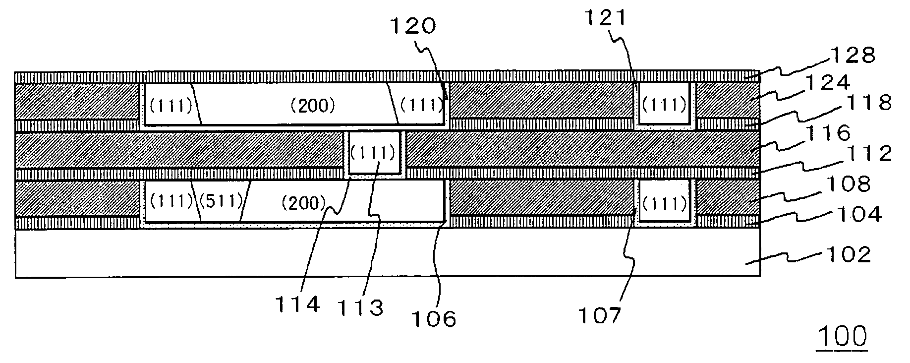
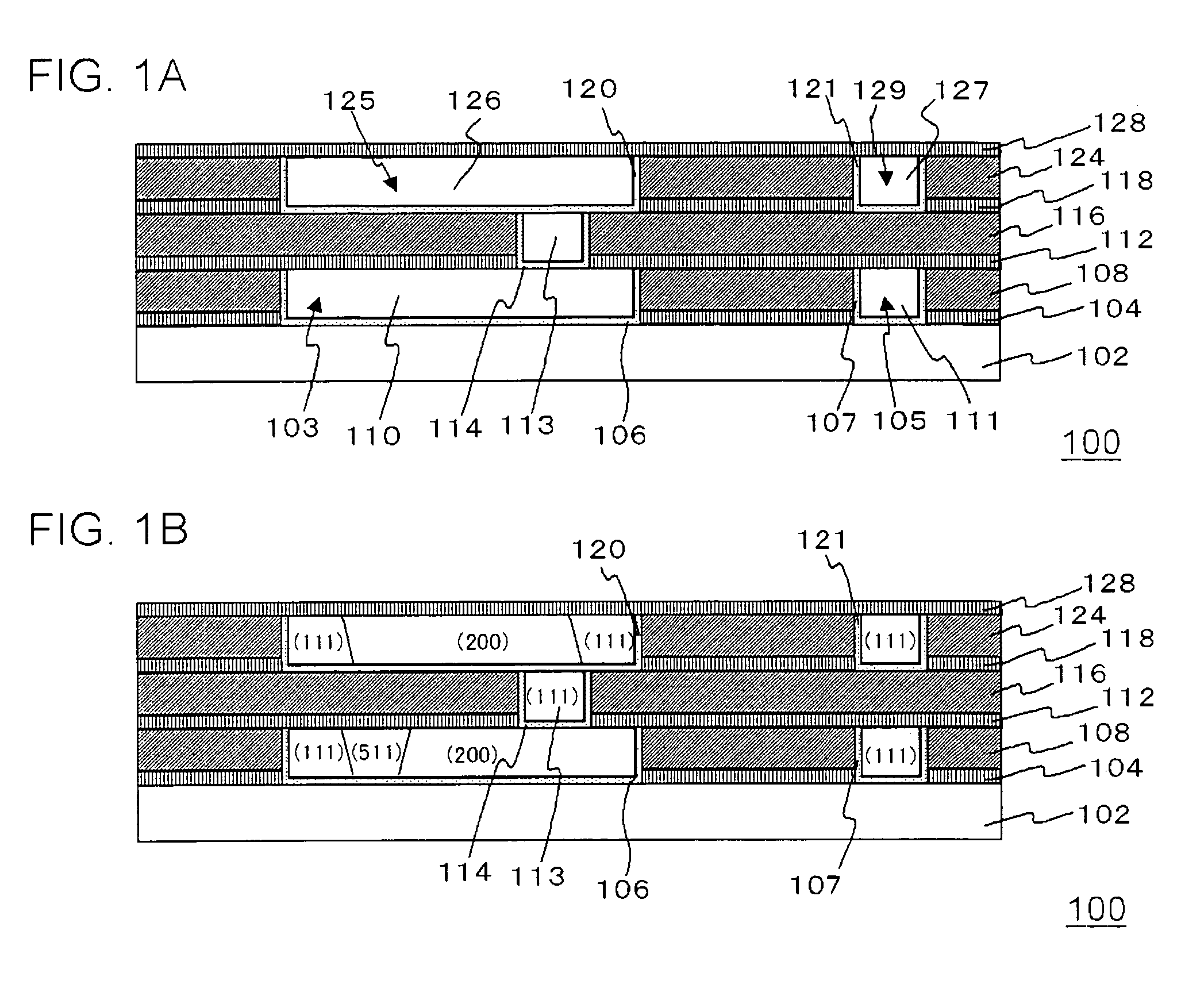
[0038]FIG. 1A is a sectional view explaining a structure of a semiconductor device 100 of this embodiment, and FIG. 1B is a sectional view explaining surface orientation of the copper interconnection of the semiconductor device 100.

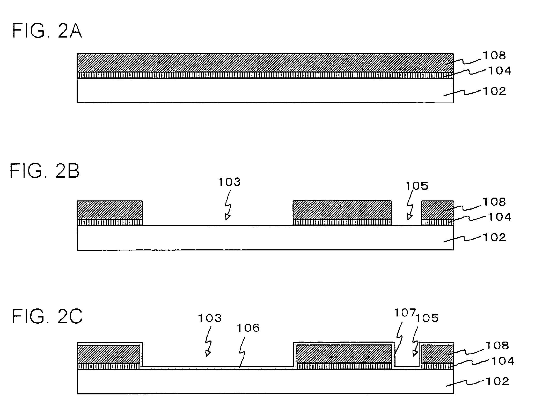
[0039]As shown in FIG. 1A, the semiconductor device 100 has a single damascene structure in which the a multi-layered copper interconnection composed of first to third layers is provided on a semiconductor substrate 102 such as a silicon substrate. A second copper interconnection 110 and a first copper interconnection 111in the first layer are configured by a second interconnect trench 103 and a first interconnect trench 105, provided in the interlayer insulating film 108 on an etching stopper film 104, having a copper film filled therein. There is a barrier metal 107, preventing Cu diffusion, placed between the interlayer insulating film 108 and the first copper interconnection 111. On the other hand, there is a barrier metal 106, preventing Cu diffusion...

second embodiment

[0076]FIGS. 7A to 7D are sectional views explaining an exemplary method of fabricating the semiconductor device 100. In this embodiment, definitions for the relatively-wide interconnect trenches, relatively-narrow interconnect trenches, aspect ratio, via diameter and width of relatively-wide interconnect trenches comply with those for the first embodiment.

[0077]First, after the process step explained in FIG. 2B in the first embodiment, a barrier metal 136 (Ta film) is formed on the interlayer insulating film 108, on the inner wall of the second interconnect trench 103, and on the inner wall of the first interconnect trench 105. This embodiment adopts a sputtering technique as a method of film formation, using a Ta target in a nitrogen gas atmosphere. Next, a seed layer (not shown) of copper is formed. Next, on the seed layer, a copper film 130 and a copper film 139 are formed by an electroplating technique (FIG. 7A). The first interconnect trench 105 herein is completely filled with...

example

Example 1

[0089]Using a method similar to that applied to the first embodiment, Ta films were formed in the relatively-narrow interconnect trenches, and TaN films were formed in the relatively-wide interconnect trenches. The copper films were buried in the narrow-width interconnect trenches by the low-current plating, and the copper films were buried in the wide-width interconnect trenches by the high-current plating. A multi-layered copper interconnection structure was fabricated so as to include the second copper interconnections having a width of as relatively wide as 10 μm were fabricated as the wide-width interconnect trenches, and the first copper interconnections having a width of as relatively narrow as 0.2 μm were fabricated as the narrow-width interconnect trenches. Most portions of the first copper interconnections were found to have (111)-surface orientation and (511)-surface orientation. Confirmation by an EBSP technique also revealed that most portions of the second cop...


PUM

PropertyMeasurementUnit
widthaaaaaaaaaa
temperatureaaaaaaaaaa
widthaaaaaaaaaa

Abstract

A semiconductor device includes: a semiconductor substrate; an insulating film provided on the semiconductor substrate; a plurality of copper interconnections provided on the same level in the insulating film. The copper interconnection includes: a first copper interconnection having a relatively narrow width; and a second copper interconnection having a relatively wide width. The first copper interconnection has the top surface thereof principally composed of copper, and the second copper interconnection has the top surface thereof principally composed of copper.

Description

[0001]This application is based on Japanese patent application No. 2004-229779 the content of which is incorporated hereinto by reference.DISCLOSURE OF THE INVENTION[0002]1. Field of the Invention[0003]The present invention relates to a semiconductor device applied with copper interconnection, and a method of fabricating the same.[0004]2. Description of the Related Art[0005]Cu interconnection is widely used in semiconductor devices in order to respond demands on faster operation of the devices. Exemplary semiconductor devices having multi-layered copper interconnection structures are described elsewhere in previous patents (Japanese Laid-Open Patent Publication No. 2001-68475, and U.S. Pat. No. 6,291,885).[0006]FIG. 10A shows a structure of a conventional Cu interconnection, and FIG. 10B shows an exemplary surface orientation of the Cu interconnection in this structure. FIGS. 10A and 10B are sectional views schematically showing a structure of a copper interconnection. The aspect ra...

Claims


Application Information

Patent Timeline
Patent Type & Authority Patents(United States)
IPC IPC(8): H01L23/48
CPCH01L21/2855H01L21/2885H01L21/76877H01L21/76883H01L21/76886H01L23/528H01L23/53228H01L23/53238H01L2924/0002H01L2924/00
Inventor TAKEWAKI, TOSHIYUKIKUNISHIMA, HIROYUKI
Owner RENESAS ELECTRONICS CORP
Why Eureka
Try Eureka