Ultraviolet light monitoring system

a monitoring system and ultraviolet light technology, applied in the direction of optical radiation measurement, semiconductor/solid-state device testing/measurement, instruments, etc., can solve the problems of light irradiation damage and become a significant problem, and achieve the effect of reducing the effect of self-aligning bias formed at the surface of the evaluation subject film and improving accuracy

Active Publication Date: 2010-06-08
LAPIS SEMICON CO LTD +1
View PDF3 Cites 0 Cited by
  • Summary
  • Abstract
  • Description
  • Claims
  • Application Information

AI Technical Summary

Benefits of technology

[0020]According to the aspect of the present invention described above, the separated first and second electrodes have an opposing structure. Thus, holes and electrons that are generated on the first and second electrodes and in the evaluation subject film between the electrodes can be captured (trapped) in a region of the gap between the first and second electrodes. As a result, effects that are caused by a self-aligning bias being formed at the surface of the evaluation subject film can be reduced, and measurements of induction current values with higher accuracy than previously are enabled.

Problems solved by technology

With the progress of miniaturization of element structures, thinning of layers and formation of three-dimensional structures in, for example, semiconductor devices, ultraviolet light irradiation damage, when ultraviolet light is emitted from a plasma which is used in a step of forming an interlayer insulation film, wiring or the like and reaches a boundary surface of a semiconductor element, has become a significant problem.

Method used


Image

  • Ultraviolet light monitoring system
  • Ultraviolet light monitoring system
  • Ultraviolet light monitoring system

Examples


first embodiment

Structure of the First Embodiment

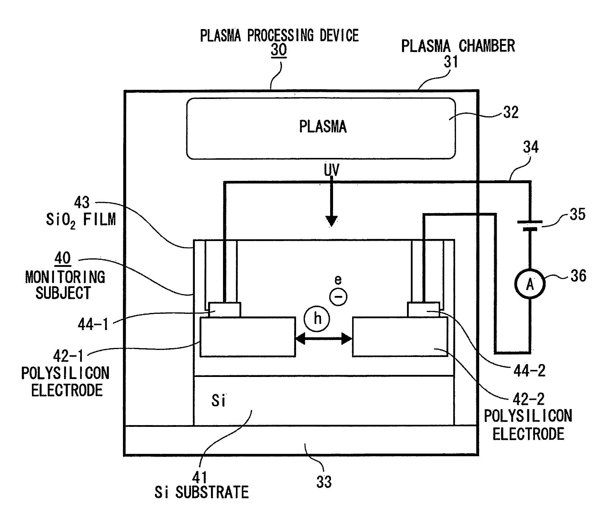
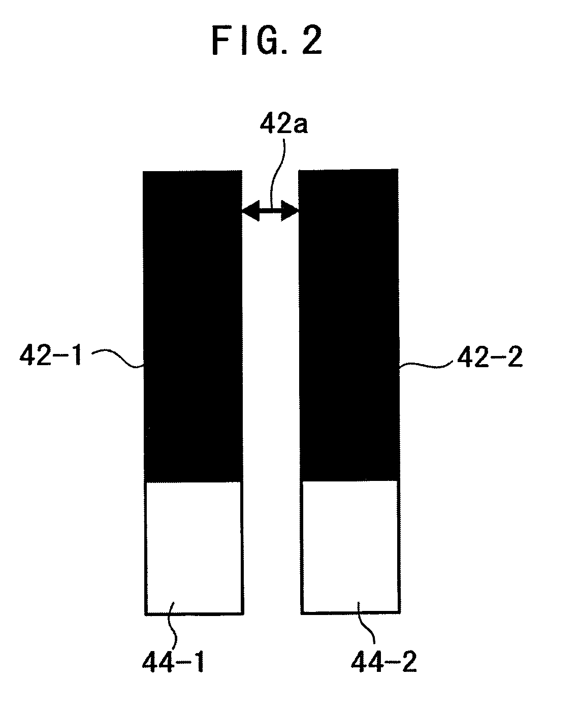
[0032]FIG. 1 is a schematic structural diagram of an ultraviolet light monitoring system (for example, a plasma monitoring system) which illustrates a first embodiment of the present invention. FIG. 2 is a schematic plan view showing electrodes of FIG. 1.

[0033]The plasma monitoring system shown in FIG. 1 is equipped with a plasma processing device 30. The plasma device 30 is an apparatus which generates plasma 32 in a plasma chamber 31, which is in a vacuum state, by application of an RF bias voltage, and implements etching, film formation or the like on a monitoring subject 40 which has been placed on a stage 33. Wiring 34 is connected to the monitoring subject 40. This wiring 34 leads out to outside the plasma chamber 31. A voltage supply 35, for applying a negative bias voltage (for example, −30 V) to the monitoring subject 40, and an ammeter 36, for measuring an induction current flowing in the monitoring subject 40, are connected in series with ...

second embodiment

Structure and Operation of the Second Embodiment

[0044]FIG. 4 is a schematic plan view showing electrodes in the monitoring subject 40 of an ultraviolet light monitoring system (for example, a plasma monitoring system) which illustrates the second embodiment of the present invention. Elements in common with elements in FIG. 2 showing the first embodiment are assigned common reference numerals.

[0045]In this second embodiment, as the first and second electrodes provided in the monitoring subject 40 of FIG. 1, there are two comb shape polysilicon electrodes 42-1A and 42-2A, which are opposed at a predetermined gap (space) corresponding to the slit 42a. These two comb shape polysilicon electrodes 42-1A and 42-2A are disposed so as to mesh with one another.

[0046]In a fabrication process of the two polysilicon electrodes 42-1A and 42-2A, when photolithography and dry etching such as plasma etching or the like are performed, for example, in the pattern formation step in which the two opposi...

third embodiment

Structure of the Third Embodiment

[0049]FIG. 5 is a schematic sectional view of a monitoring subject in an ultraviolet light monitoring system (for example, a plasma monitoring system) which illustrates a third embodiment of the present invention. Elements in common with elements in FIG. 1 and FIG. 3I showing the first embodiment are assigned common reference numerals.

[0050]In the plasma monitoring system of this third embodiment, instead of the monitoring subject 40 of the first embodiment shown in FIG. 1, a monitoring subject 40B with a different structure is employed. The monitoring subject 40B includes the silicon substrate 41, and the two polysilicon electrodes 42-1 and 42-2, which are first and second electrodes, are formed on the silicon substrate 41 with the thermal oxide film 51 therebetween. Similarly to the first embodiment, the two polysilicon electrodes 42-1 and 42-2 are opposingly disposed with the slit 42a with the predetermined gap therebetween. However, differently f...


PUM


Abstract

An ultraviolet light monitoring system includes first and second electrodes, an evaluation subject film and a power source. The first and second electrodes are opposingly disposed and attract holes which are generated in accordance with irradiation of ultraviolet light. The evaluation subject film is formed in a vicinity of the first and second electrodes, and is a subject of evaluation of damage caused by the irradiation of ultraviolet light. The power source, at times of monitoring of the ultraviolet light, applies a predetermined bias to a series path formed by the first electrode, a gap between the first and second electrodes, and the second electrode.

Description

CROSS-REFERENCE TO RELATED APPLICATION[0001]This application claims priority under 35 USC 119 from Japanese Patent Application No. 2007-225676, the disclosure of which is incorporated by reference herein.BACKGROUND OF THE INVENTION[0002]1. Field of the Invention[0003]The present invention relates to an ultraviolet light monitoring system that quantitatively and in real time monitors damage caused by ultraviolet light from plasma or the like in a semiconductor fabrication step (process) or the like.[0004]2. Description of the Related Art[0005]With the progress of miniaturization of element structures, thinning of layers and formation of three-dimensional structures in, for example, semiconductor devices, ultraviolet light irradiation damage, when ultraviolet light is emitted from a plasma which is used in a step of forming an interlayer insulation film, wiring or the like and reaches a boundary surface of a semiconductor element, has become a significant problem.[0006]As a countermea...

Claims


Application Information

Patent Timeline
Patent Type & Authority Patents(United States)
IPC IPC(8): G01J1/10
CPCH01L22/14H01L2924/0002H01L2924/00
Inventor HASHIMOTO, JUNKAWADA, SHINJIKURACHI, IKUOSAMUKAWA, SEIJI
Owner LAPIS SEMICON CO LTD
Why Eureka
Try Eureka