Stacked pixel for high resolution CMOS image sensor

a stacked, image sensor technology, applied in the field of solid-state image sensors, can solve the problems of sacrificing resolution, reducing the resolution of stacked pixels, and reducing the number of transistors in each pixel, so as to achieve the effect of reducing the loss of light sensitivity, reducing the loss of resolution, and simplifying and more practical solutions

Active Publication Date: 2010-06-15
INTELLECTUAL VENTURES II
View PDF26 Cites 16 Cited by
  • Summary
  • Abstract
  • Description
  • Claims
  • Application Information

AI Technical Summary

Benefits of technology

[0010]It is an object of the present invention to provide a CMOS image sensor with stacked photo-sites, which sense color by vertically separating photo-generated carriers, so that the CMOS image sensor has an advantage of providing two or more color-coded signals without using conventional light absorbing color filters. Placing suitable potential barriers under a typical pinned photodiode structure achieves this goal and other objects of the invention.
[0013]The above described exemplary embodiments of the present invention address usual difficulties and provide a simpler and more practical solution for color sensing with less resolution loss than in the typical approach and with minimum loss of light sensitivity. For instance, U.S. Pat. No. 6,894,265 issued to Richard B. Merrill et al. teaches one typical approach of forming the buried photodiode and collecting and storing charge in the deep silicon bulk. On the contrary to the typical approach, a special potential barrier is placed under the standard pinned photodiode, and thus, it is possible do divert the photo-generated carriers from the deep bulk and direct the photo-generated carriers to flow in a narrow region to the surface of the silicon substrate where the photo-generated carriers can be easily collected and stored for readout.
[0014]The carriers from the bulk can thus be conveniently stored in a suitable structure next to the carriers generated and stored in the standard photodiode near the silicon substrate surface. It is thus not necessary to form buried photodiodes and collect and store charge deep in the bulk of the silicon, which is often difficult to access, read, and reset. It is also possible to place the special potential barrier in different depths in different pixels and thus make the pixels sensitive to different light spectral regions. Each pixel can thus provide two or more differently coded color signals instead of one. The resolution is not sacrificed as much as in the typical approach and the light sensitivity is also not sacrificed, since no color absorbing filters or not as many color absorbing filters are used. Storing all the photo-generated charge close to the silicon surface makes possible to share some of the low noise readout and reset circuitry that is located there and thus achieve high performance with very small pixel sizes. This approach is thus much simpler and easier to implement in the current CMOS technology with high yield.

Problems solved by technology

The larger number of transistors in each pixel may become a disadvantage when the pixel size needs to be reduced in order to build low cost and high-resolution image sensors.
All these approaches to the color sensing may have a principal disadvantage of sacrificing the resolution as mentioned above and sacrificing sensitivity by absorbing light in color filters.
While functioning well, this pixel has no ability to separate charge according to the depth of charge generation and thus according to the wavelength of the photons that have created the charge.
The absorption of light causes loss of sensitivity, which is an unwanted side effect of this method of color sensing.
However, it may not be easy to form the photodiodes that are buried deeply in the silicon bulk.
Also, it may be difficult to sense charge collected in the buried photodiodes by circuits located on top of the silicon without adding noise.

Method used


Image

  • Stacked pixel for high resolution CMOS image sensor
  • Stacked pixel for high resolution CMOS image sensor
  • Stacked pixel for high resolution CMOS image sensor

Examples


first embodiment

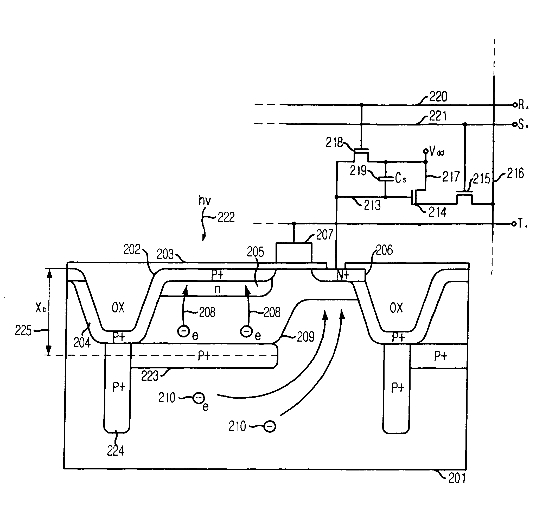
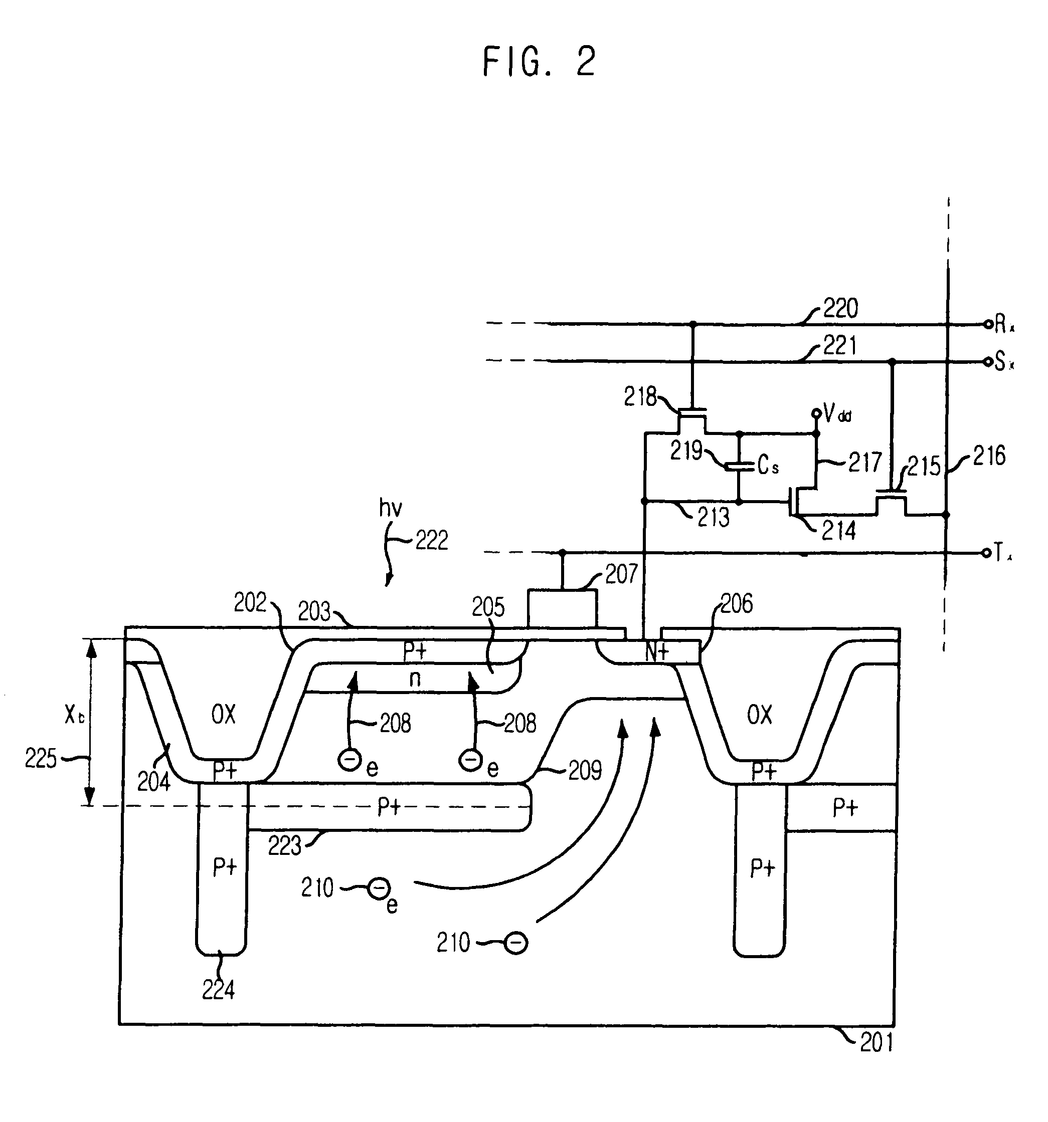
[0027]FIG. 2 is a simplified cross-sectional view illustrating a pixel with a stacked photo-site and a potential barrier and readout circuits associated with the pixel in accordance with the present invention.

[0028]According to the first embodiment of the present invention, the pixel has an ability to separate charge according to the depth of charge generation and thus sense color. A substrate 201 has a shallow STI region 202, obtained by forming a trench through etching the substrate 201 to a certain depth and filling the trench with a silicon dioxide layer 203. The silicon dioxide layer 203 also covers the entire surface of the pixel. Herein, the substrate 201 is a p-type silicon substrate. A shallow p+-type doped region 204 passivates the walls and the bottom of the STI region 202 as well as the surface of the pixel to minimize a dark current generation. However, in this pixel, a p+-type doped barrier 223 is placed into the pixel at a depth Xb 225. This p+-type doped barrier 223 ...

second embodiment

[0034]There are many other combinations of the pinned photodiode arrangements and charge storage wells that can be used with the pixel according to the present invention. For the simplicity of description one such possibility and another embodiment of the present invention is shown only in a simplified circuit diagram form in FIG. 4.

[0035]FIG. 4 is a simplified circuit diagram illustrating a stacked pixel where charge from a shallow depleted region is stored in a pinned photodiode 401 and charge from a deep undepleted region is directed to another pinned photodiode 402. The pinned photodiodes 401 and 402 interface with a common FD charge detection node 408 via respective charge transfer gates 403 and 404. The rest of the circuit is the same as in the first and second embodiments where transistors 405, 406 and 407 are a SF transistor 405, an address transistor and a reset transistor, respectively. Control signals are supplied to the pixel via a reset gate bus Rx 410, an address gate ...


PUM


Abstract

Provided is a solid-state CMOS image sensor, specifically a CMOS image sensor pixel that has stacked photo-sites, high sensitivity, and low dark current. In an image sensor including an array of pixels, each pixel includes: a standard photo-sensing and charge storage region formed in a first region under a surface portion of a substrate and collecting photo-generated carriers; a second charge storage region formed adjacent to the surface portion of the substrate and separated from the standard photo-sensing and charge storage region; and a potential barrier formed between the first region and a second region underneath the first region and diverting the photo-generated carriers from the second region to the second charge storage region.

Description

FIELD OF THE INVENTION[0001]The present invention relates to a solid-state image sensor; and, more particularly to a complementary metal oxide semiconductor (CMOS) image sensor with stacked photo-sites, which result in a compact pixel layout, high sensitivity, and low dark current. The vertical photo-site arrangement obviates the need for utilization of standard light-absorbing color filters to sense colors and increases the sensor pixel density.DESCRIPTION OF RELATED ARTS[0002]Typical image sensors sense light by converting impinging photons into electrons that are integrated (collected) in sensor pixels. After completion of an integration cycle, collected charge is converted into a voltage, which is supplied to output terminals of the sensor. In a CMOS image sensor, charge-to-voltage conversion is accomplished directly in the pixels themselves and the analog pixel voltage is transferred to the output terminals through various pixel addressing and scanning schemes. The analog signa...

Claims


Application Information

Patent Timeline
Patent Type & Authority Patents(United States)
IPC IPC(8): H01L31/113H01L27/14H01L27/146H04N5/335H04N5/369H04N5/374H04N5/3745H04N9/07
CPCH01L27/14609H01L27/14621H01L27/1463H01L27/14643H01L27/14632H01L27/14627H01L27/146
Inventor HYNECEK, JAROSLAV
Owner INTELLECTUAL VENTURES II
Why Eureka
Try Eureka