Oxygen-rich layers underlying BPSG

a technology of oxygen-rich layers and bpsg, which is applied in the direction of semiconductor devices, semiconductor/solid-state device details, electrical apparatus, etc., can solve the problems of electrical property shift, failure of devices, and worsening of integrated circuits, so as to improve the gap filling ability of dielectric layers and reduce lateral etching

Active Publication Date: 2010-06-22
TAIWAN SEMICON MFG CO LTD
View PDF9 Cites 3 Cited by
  • Summary
  • Abstract
  • Description
  • Claims
  • Application Information

AI Technical Summary

Benefits of technology

[0012]The advantageous features of the present invention include improved gap filling ability of dielectric layers and reduced lateral etching in the dielectric layer.

Problems solved by technology

This situation becomes worse in integrated circuits formed using 90 nm technology or below.
In addition, boron and phosphorous may penetrate into devices, resulting the electrical property shift and even the failure of the devices.

Method used


Image

  • Oxygen-rich layers underlying BPSG
  • Oxygen-rich layers underlying BPSG
  • Oxygen-rich layers underlying BPSG

Examples


Embodiment Construction

[0016]The making and using of the presently preferred embodiments are discussed in detail below. It should be appreciated, however, that the present invention provides many applicable inventive concepts that can be embodied in a wide variety of specific contexts. The specific embodiments discussed are merely illustrative of specific ways to make and use the invention, and do not limit the scope of the invention.

[0017]A novel method for forming dielectric layers is provided. The intermediate stages of manufacturing a preferred embodiment of the present invention are illustrated. The variations of the preferred embodiment are then discussed. Throughout the various views and illustrative embodiments of the present invention, like reference numbers are used to designate like elements.

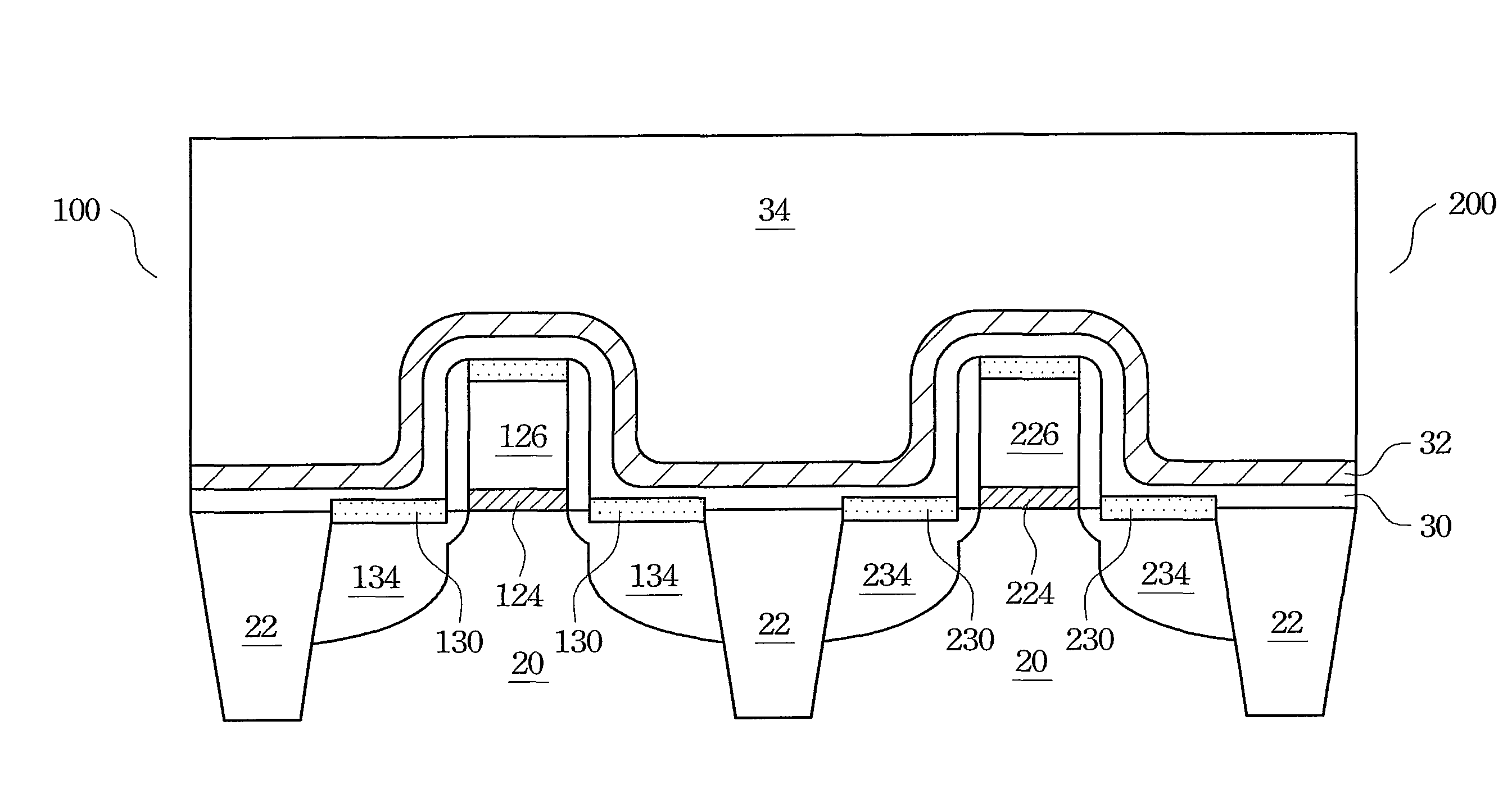
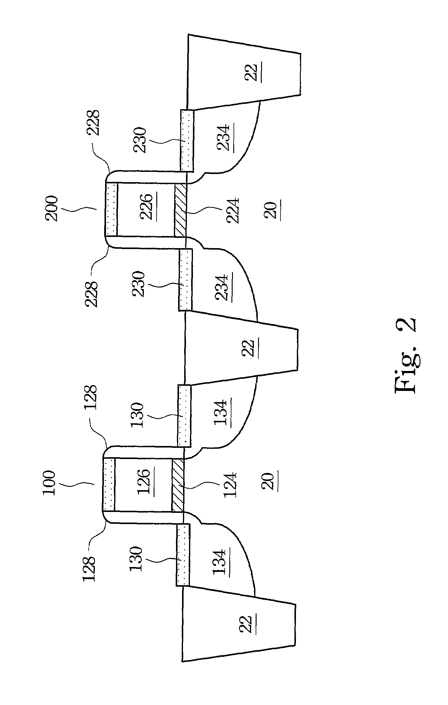
[0018]FIGS. 2 though 7 illustrate cross-sectional views of an embodiment of the present invention. Referring to FIG. 2, substrate 20 is provided. Substrate 20 is preferably a semiconductor substrate, which ...


PUM


Abstract

An integrated circuit structure and a method of forming the same are provided. The method includes providing a surface; performing an ionized oxygen treatment to the surface; forming an initial layer comprising silicon oxide using first process gases comprising a first oxygen-containing gas and tetraethoxysilane (TEOS); and forming a silicate glass over the initial layer. The method may further include forming a buffer layer using second process gases comprising a second oxygen-containing gas and TEOS, wherein the first and the second process gases have different oxygen-to-TEOS ratio.

Description

TECHNICAL FIELD[0001]This invention relates generally to integrated circuits, and more particularly to the formation of dielectric layers underlying boron and / or phosphorous containing silicate glass.BACKGROUND[0002]In modern integrated circuits, semiconductor devices are formed on semiconductor substrates, and are connected through metallization layers. The metallization layers are interconnected to the semiconductor devices through contact plugs. Also, external pads are connected to the semiconductor devices through the contact plugs.[0003]The metallization layers are separated from each other by dielectric layers. Further, the metallization layers are separated from active devices by an inter-layer dielectric (ILD). Conventionally, the dielectric layers, particularly the ILDs, are often formed of boronphosphosilicate glass (BPSG).[0004]FIG. 1 illustrates a conventional structure. Transistors 4, which include gates 16 and source / drain regions 14, are formed at the surface of semic...

Claims


Application Information

Patent Timeline
Patent Type & Authority Patents(United States)
IPC IPC(8): H01L21/8238
CPCH01L21/02129H01L21/02164H01L21/02271H01L21/02304H01L21/76837H01L21/31612H01L21/321H01L21/76826H01L21/76832H01L21/3105
Inventor JANGJIAN, SHIU-KOHUANG, WAN-TINGCHIEN, YU-JENSUN, PHIL
Owner TAIWAN SEMICON MFG CO LTD
Why Eureka
Try Eureka