Pattern defect inspection apparatus and method

a technology of defect detection and inspection apparatus, applied in the direction of optically investigating flaws/contamination, semiconductor/solid-state device testing/measurement, instruments, etc., can solve the problems of impeded difficult detection of target defects, and non-uniform intensity of interference light intensity

Inactive Publication Date: 2010-06-29
HITACHI HIGH-TECH CORP
View PDF8 Cites 4 Cited by
  • Summary
  • Abstract
  • Description
  • Claims
  • Application Information

AI Technical Summary

Benefits of technology

[0012]Development of high NA of an objective lens for inspection and optical super resolution technology has been made as the optical inspection technology. However, because the high NA of the objective lens for inspection has reached a physical limit, an essential approach is to reduce the wavelength of illumination light to UV (Ultra Violet) light and DUV (Deep Ultra Violet) light. To increase light power of the rays of light emitted from a minute target defect, on the other hand, an illumination light source having high luminance is necessary. Therefore, a laser beam source is used in many cases as the illumination light source to acquire illumination light having high luminance in the UV and DUV ranges.
[0014]It is therefore an object of the invention to accomplish pattern defect inspection apparatus and method capable of detecting highly precisely minute defects on a sample without generating speckle noise in signals.
[0019]The invention can accomplish pattern defect inspection apparatus and method capable of detecting highly precisely minute defects on a sample without generating speckle noise in signals.

Problems solved by technology

Consequently, detection of the target defect has become more difficult.
Factors that impede the detection of the target defect include grains of metal wires such as aluminum, minute concavo-convexities of a surface called “morphology”, non-uniformity of the intensity of interference light due to a very small difference of the film thickness of transparent films (transparent to an illumination wavelength) such as an insulating film, roughness of edge portions of wiring, and so forth.
However, because the high NA of the objective lens for inspection has reached a physical limit, an essential approach is to reduce the wavelength of illumination light to UV (Ultra Violet) light and DUV (Deep Ultra Violet) light.
When the laser beam source having such high luminance is used in the prior art technology, however, speckle noise owing to interference of illumination light such as the laser beam source invites the increases of variance of signals detected by detectors and results in noise during signal processing.
Consequently, a minute defect cannot be detected highly precisely.

Method used


Image

  • Pattern defect inspection apparatus and method
  • Pattern defect inspection apparatus and method
  • Pattern defect inspection apparatus and method

Examples


first embodiment

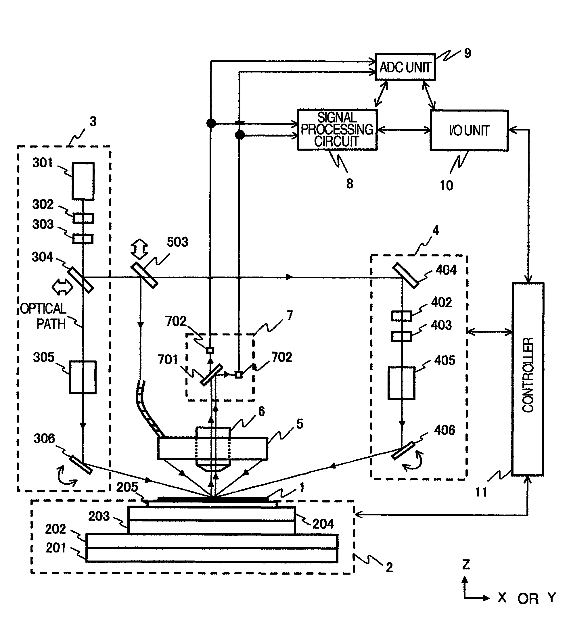
[0046]FIG. 1 is a schematic structural view of a pattern defect inspection apparatus according to the first embodiment of the invention. The invention will be hereinafter explained about the case where it is applied to the inspection of a semiconductor wafer by way of example.

[0047]Referring to FIG. 1, the pattern defect inspection apparatus includes a conveying system 2 for supporting and moving a wafer 1 as an inspection object, illuminating units 3 and 4, a multi-direction illuminating unit 5, an objective lens 6, a multi-region detecting unit 7, a signal processing circuit 8, an ADC (Automatic Defect Classification) unit 9, an input / output unit 10, a controller 11 for each unit and relay lenses and mirrors that are not shown in the drawing. Incidentally, arrows (part of which is not shown) extending from the controller 11 to each unit represents that control signals, etc, are mutually communicated.

[0048]Next, the operation will be explained. Beams of illumination light emitted f...

second embodiment

[0101]Next, the second embodiment of the invention will be explained. In this second embodiment, the construction of the illuminating units 3 and 4 of the defect inspection apparatus is different from the construction in the first embodiment. Since the rest of the constructions are the same, their detailed explanation will be omitted.

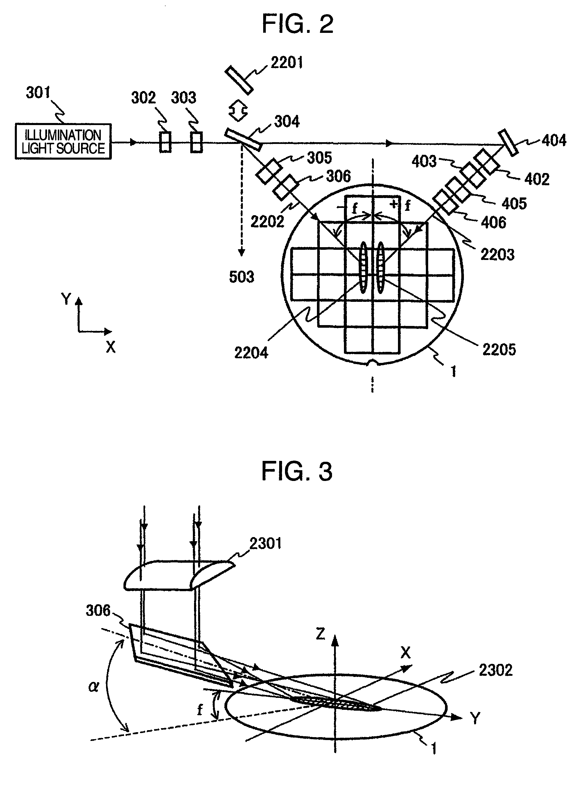
[0102]FIG. 13 shows the construction of the illumination of the second embodiment for illuminating a plurality of regions on the wafer 1. The difference of the example shown in FIG. 13 from that of FIG. 2 resides in that whereas illumination is made from if directions with respect to the X or Y direction of the conveying system 2 in the example shown in FIG. 2, it is made from the same direction, that is, from the direction of f=0 in the example shown in FIG. 13.

[0103]The advantage of the construction of the illuminating unit shown in FIG. 13 is that the size of the construction of the apparatus can be reduced because the illumination direction and the ...

third embodiment

[0105]Next, the third embodiment of the invention will be explained. In the third embodiment, the construction of the illuminating unit 3 of the defect inspection apparatus is different from the construction in the first embodiment. Since the rest of the constructions are the same, their detailed explanation will be omitted.

[0106]FIG. 14 shows a schematic construction of the illuminating unit in this third embodiment. The third embodiment uses a plurality of light sources of the illuminating unit. In FIG. 14, an illumination light source 3401 of a wavelength λ2 different from the wavelength λ1 of the illumination light source 301, a light power polarization adjusting unit 3402, a coherency reducing unit 3403, a condensation optical system 3405 and an oblique illumination mirror 3406 are arranged in place of the illuminating unit 4.

[0107]The functions of the light power polarization adjusting unit 3402, the coherency reducing unit 3403, the condensation optical system 3405 and the ob...


PUM

PropertyMeasurementUnit
wavelengthaaaaaaaaaa

Abstract

A pattern defect inspection apparatus capable of detecting minute defects on a sample with high sensitivity without generating speckle noise in signals is realized. Substantially the same region on a surface of a wafer is detected by using two detectors at mutually different timings. Output signals from the two detectors are summed and averaged to eliminate noise. Since a large number of rays of illumination light are not simultaneously irradiated to the same region on the wafer, a pattern defect inspection apparatus capable of suppressing noise resulting from interference of a large number of rays, eliminating noise owing to other causes and detecting with high sensitivity minute defects on the sample without the occurrence of speckle noise in the signal can be accomplished.

Description

BACKGROUND OF THE INVENTION[0001]1. Field of the Invention[0002]This invention relates to a pattern defect inspection apparatus for detecting defects and foreign matters of a circuit pattern on a sample.[0003]2. Description of the Related Art[0004]Foreign matters and defects (short-circuit, wire breakage, etc) on a semiconductor wafer, if any, will result in insulation defects and short-circuits of wires and capacitors and film breakage of gate oxide films and eventually, in the defects of semiconductor devices in semiconductor production processes.[0005]Structures of semiconductor devices have got more and more diversified and complicated in recent years. Semiconductor devices are classified into memory products that are constituted mainly of repetition patterns and logic products that are constituted mainly of non-repetition patterns, for example. Since product life of the semiconductor device products is relatively short, the production yield must be improved within a short perio...

Claims


Application Information

Patent Timeline
Patent Type & Authority Patents(United States)
IPC IPC(8): G01N21/00G01N21/956H01L21/66
CPCG01N21/95607G01N21/9501G01N21/94G01N2021/4711
Inventor NISHIYAMA, HIDETOSHISHIMURA, KEIUTO, SACHIONOGUCHI, MINORI
Owner HITACHI HIGH-TECH CORP
Why Eureka
Try Eureka