Method for lithography for optimizing process conditions

a technology of process conditions and lithography, applied in the field of lithography, can solve the problems of limited throughput, inability to meet the aggressive resolution targets of future generation products, and inability to use conventional optical projection lithography

Inactive Publication Date: 2010-08-03
GLOBALFOUNDRIES INC
View PDF4 Cites 8 Cited by
  • Summary
  • Abstract
  • Description
  • Claims
  • Application Information

AI Technical Summary

Problems solved by technology

As pattern resolution requirements become ever more demanding, conventional optical projection lithography is unable to meet the aggressive resolution targets required for future generation products.
However, its throughput is limited due to the serial nature of the patterning and high vacuum requirement.
However, the single chemical resist use in the process must be sensitive to both radiation sources, for example, photon and electron exposure.

Method used


Image

  • Method for lithography for optimizing process conditions
  • Method for lithography for optimizing process conditions

Examples


Embodiment Construction

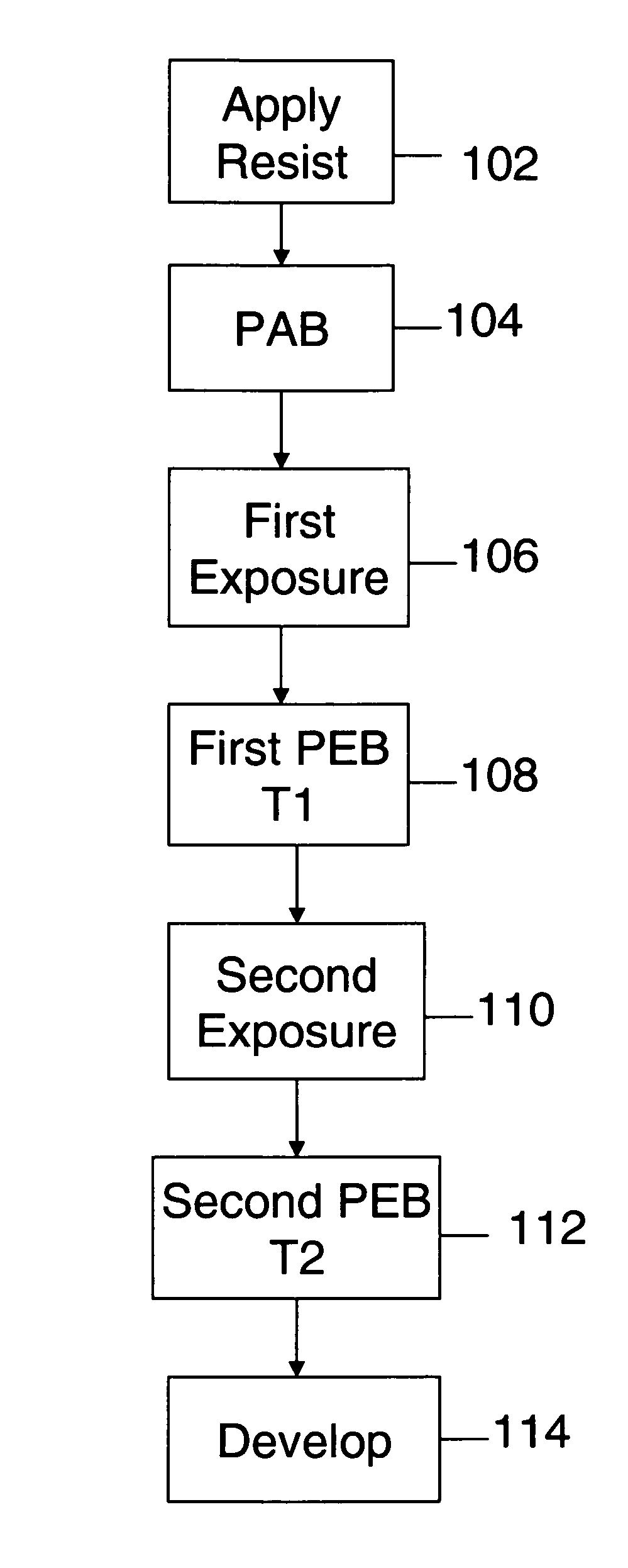
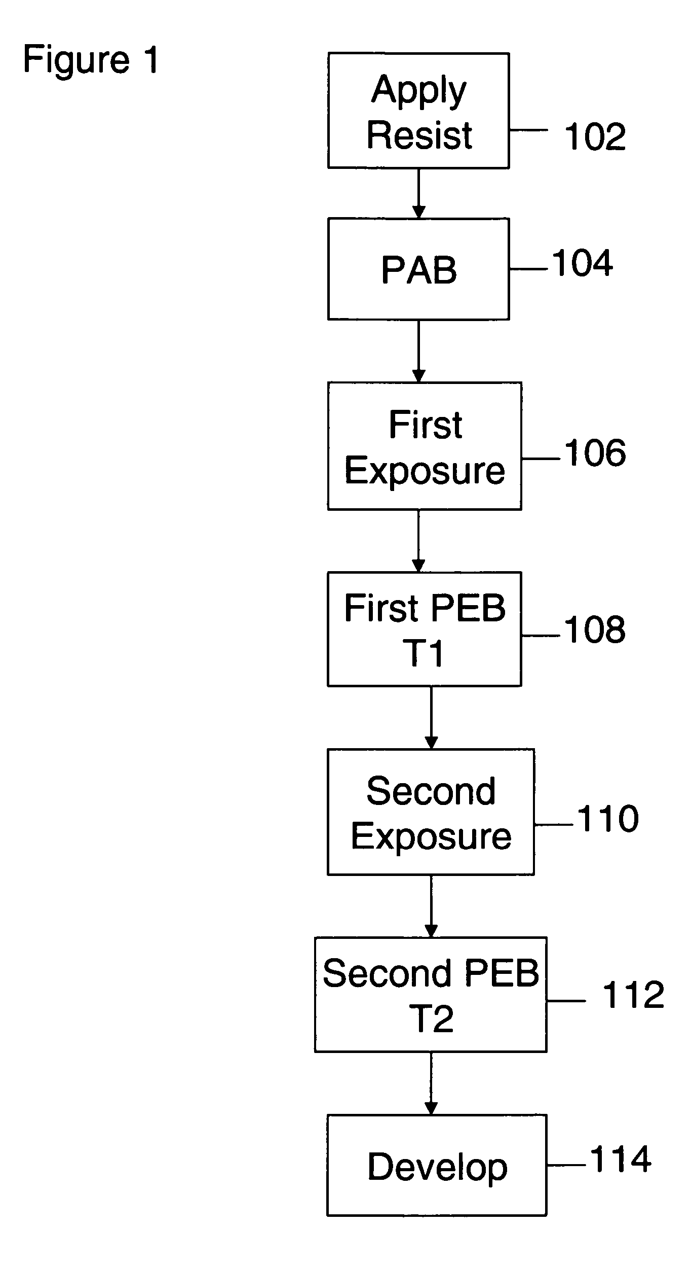
[0011]The present invention relates to a method of lithography, and in particular, a method for optimizing process conditions for lithography that involves a sequential exposure of a single resist layer by one or more radiation sources.

[0012]The invention is applicable to hybrid lithography using resists that require a post-exposure bake (PEB), e.g., chemically amplified resists used in semiconductor manufacturing. The post-exposure bake, which is performed after the resist is exposed to certain radiation, provides thermal activation that amplifies the chemical reaction induced by irradiation. The amplification gives rise to the high sensitivity for chemically amplified resists. The present invention provides for a different post-exposure bake for each exposure step, which allows the resist to be processed at different sensitivities. Thus, processing conditions of the resist for each radiation source can be independently optimized.

[0013]This process is applicable to lithography invo...


PUM

PropertyMeasurementUnit
radiation wavelengthaaaaaaaaaa

Abstract

A method of lithography is disclosed, which allows for independent resist process optimization of two or more exposure steps that are performed on a single resist layer. By providing for a separate post-exposure bake after each resist exposure step, pattern resolution for each exposure can be optimized. The method can generally be used with different lithographic techniques, and is well-suited for hybrid lithography. It has been applied to the fabrication of a device, in which the active area and the gate levels are defined in separate mask levels using hybrid lithography with an e-beam source and a 248 nm source respectively. Conditions for post-exposure bakes after the two exposure steps are independently adjusted to provide for optimized results.

Description

FIELD OF THE INVENTION[0001]The invention relates generally to a method of lithography and more particularly, to a method for optimizing process conditions in lithography with two or more exposure steps in a single mask level.BACKGROUND OF THE INVENTION[0002]Optical projection lithography is a high resolution technique currently used for defining circuits in the semiconductor industry. As pattern resolution requirements become ever more demanding, conventional optical projection lithography is unable to meet the aggressive resolution targets required for future generation products. Parallel development is underway to enhance traditional optical projection lithography, for example, using immersion schemes, as well as to explore alternative shorter wavelength radiation sources that may provide higher resolution patterning such as extreme ultra-violet (EUV), as well as electron or ion beam based schemes and, to a certain degree, x-ray radiation.[0003]Before advanced manufacturing litho...

Claims


Application Information

Patent Timeline
Patent Type & Authority Patents(United States)
IPC IPC(8): G03F7/20
CPCG03F7/2022
Inventor LARSON, CARL E.MCNAB, SHAREE J.STEEN, STEVEN E.VISWANATHAN, RAMAN G.WALLRAFF, GREGORY M.
Owner GLOBALFOUNDRIES INC
Why Eureka
Try Eureka