Method of manufacturing semiconductor device

a manufacturing method and semiconductor technology, applied in the direction of semiconductor devices, basic electric elements, electrical equipment, etc., can solve the problems of increasing the difficulty of capacitance contact plug formation, reducing the area allowed for each component element, and increasing the difficulty of forming each of the above-described contact plugs

Active Publication Date: 2010-08-03
HEFEI RELIANCE MEMORY LTD
View PDF36 Cites 2 Cited by
  • Summary
  • Abstract
  • Description
  • Claims
  • Application Information

AI Technical Summary

Benefits of technology

[0021]According to the present invention, a sacrificial interlayer film made of amorphous carbon is formed, with a top surface and side surfaces of a bit line, which is formed on a second interlayer insulating film formed on a first contact plug, covered with silicon nitride. Because amorphous carbon can be dry etched with a gas which does not contain halogen gases, such as oxygen, hydrogen and ammonia, it is possible to form a contact hole in the amorphous carbon without etching in the last the silicon nitride film covering the bit line. Therefore, it becomes possible to cause silicon nitride film having a sufficient thickness to remain on the bit line and this provides the advantage that it is possible to prevent the contact plug and the bit line from forming a short circuit. Also, after the formation of the contact plug, it is possible to selectively remove only the amorphous carbon without exerting an adverse effect on the other structures by using oxygen or the like. After that, it is possible to form an interlayer insulating film made of silicon oxide so as to cover the contact plug and, therefore, this provides the advantage that the succeeding capacity formation step can be performed by using conventional techniques.

Problems solved by technology

For this reason, also the plane area allowed for each component element must be decreased and the formation of each of the above-described contact plugs has also become very difficult.
In particular, in the formation of the capacitance contact plug (the third contact plug) formed between adjacent bit lines (the second interconnect layer), it is necessary to increase the thickness of the interlayer insulating film which insulates the bit line and the capacitor in order to ensure the fabrication margin of the capacitor, and for this reason, the working margin becomes small, thereby bringing the formation of the capacitance contact plug into a more difficult situation.
However, with progress in miniaturization, it has become difficult to form high-reliability contact holes even by use of the above-described SAC method.
The etching rate ratio between silicon oxide and silicon nitride in dry etching is 5 to 7 or so, and it is difficult to dramatically change this value even by changing dry etching conditions.
This is because both silicon oxide and silicon nitride are silicon compounds and in an environment of dry etching it is difficult to expand the difference in the etching rate.
However, when the contact hole diameter decreases, the deeper a contact hole, the lower the etching rate will be and it becomes impossible to maintain the above-described etching rate ratio.
As the result, the silicon nitride film having a thickness of 60 nm formed on the bit line is completely etched before the surface of the first contact plug 108 is exposed, thereby posing the problem that the third contact plug 113 and the bit line 111 form a short circuit in the part indicated by a circle mark A. Although this problem can be solved to a certain extent by increasing the thickness of the silicon nitride film, another problem will arise; for example, the formation of the third interlayer insulating film 112 will undesirably become difficult.

Method used


Image

  • Method of manufacturing semiconductor device
  • Method of manufacturing semiconductor device
  • Method of manufacturing semiconductor device

Examples


embodiment 1

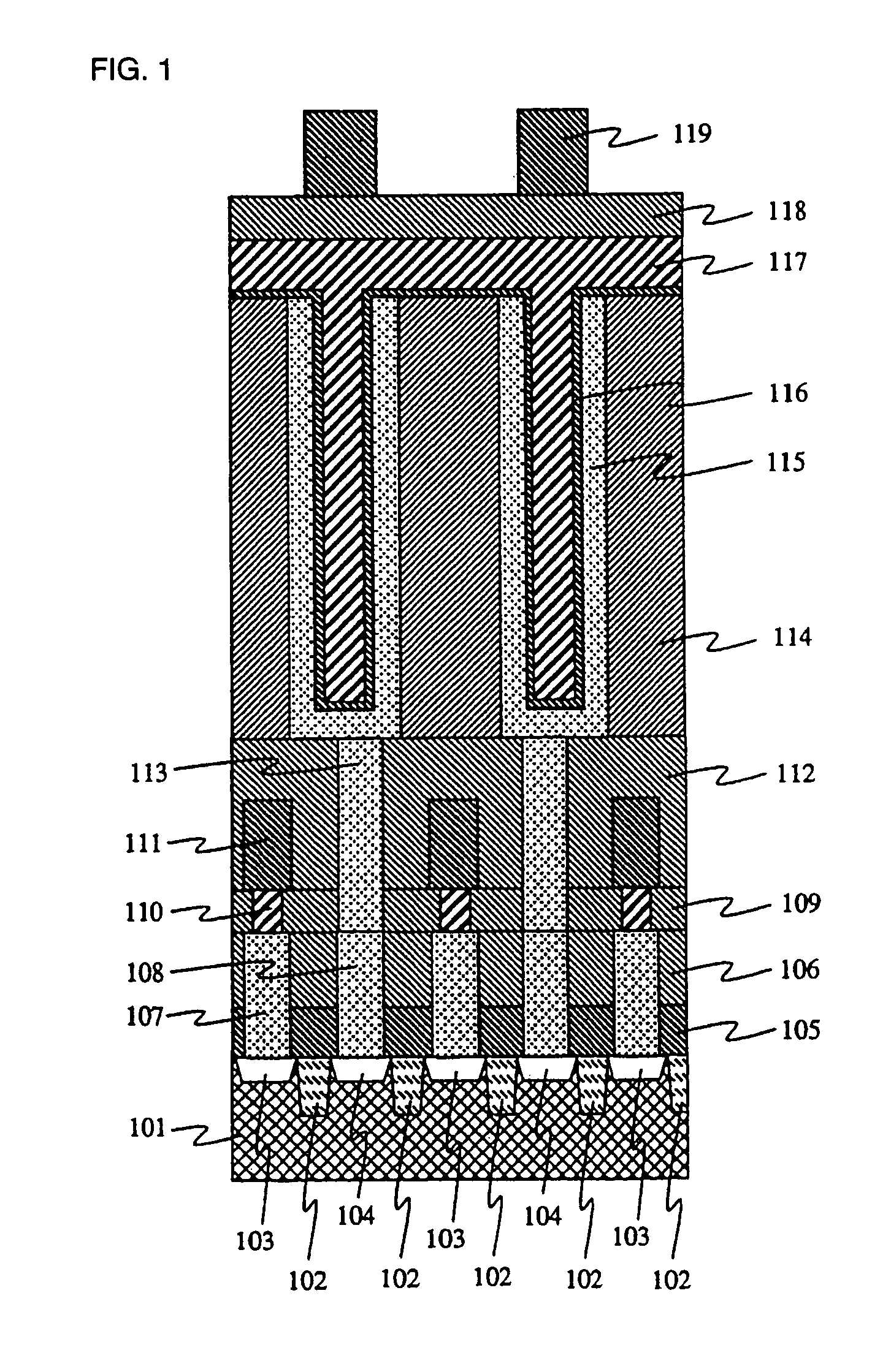
[0028]First, a description will be given of the first embodiment of the present invention, in which amorphous carbon is used for a sacrificial interlayer film which forms a contact hole, by using the sectional views of a series of steps shown in FIGS. 3A to 3K. Incidentally, the steps until the formation of a first interconnect layer which forms a word line are omitted.

[0029]First, as shown in FIG. 3A, first contact plugs 107 and 108, which are made of polycrystalline silicon, were formed in a prescribed region of a first interlayer insulating film 106 made of silicon oxide, a second interlayer film 109 which consists of a silicon oxide film having a thickness of 150 nm was formed on top of the first contact plugs, and a second contact plug, which becomes a bit line contact plug, was formed in a prescribed region of the second interlayer insulating film. The bit line contact plug can be formed by burying titanium nitride and tungsten by use of the CVD (Chemical Vapor Deposition) met...

embodiment 2

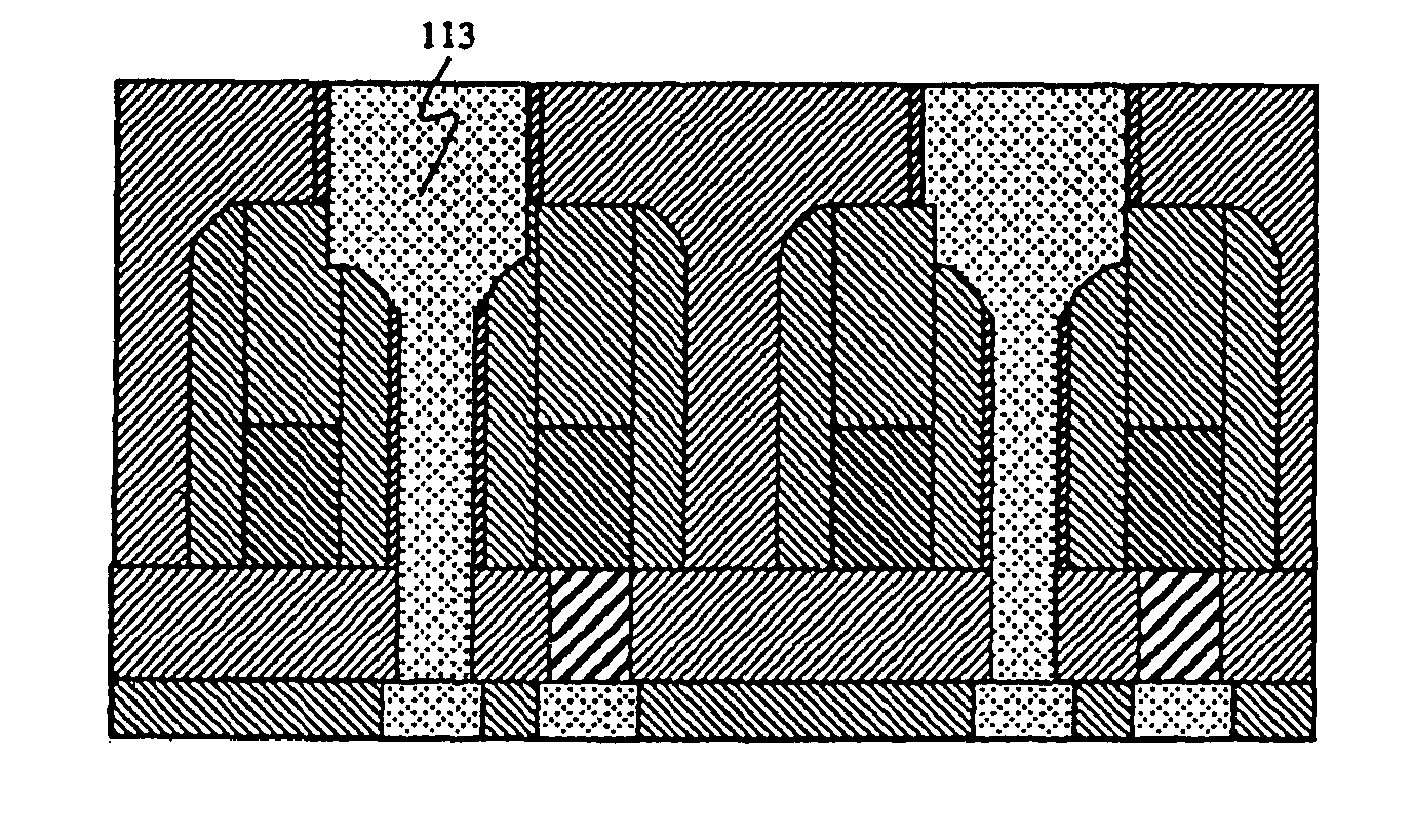
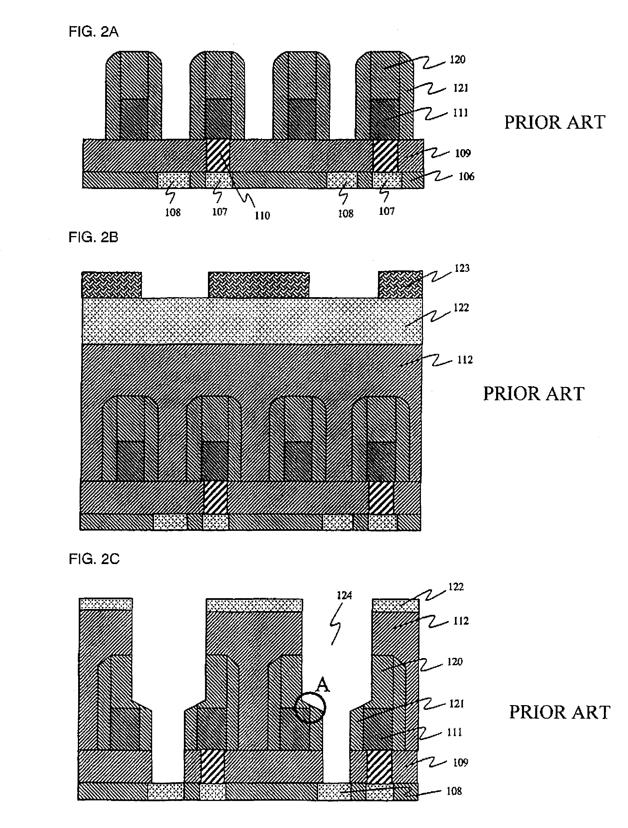
[0042]In the above-described first embodiment, after the formation of the contact hole in the amorphous carbon film and in the second interlayer insulating film, the third contact plug which consists of a silicon film was formed. Because the amorphous carbon film is formed by the plasma CVD method, the step coverage becomes a little worse. For example, if the amorphous carbon film is formed so as to cover the bit lines which are densely arranged, it is impossible completely bury the spacing between adjacent bit lines, whereby the occurrence of voids is feared. If the voids occur, the silicon film is formed in the voids and this may give rise to the problem that the adjacent contact plugs form a short circuit.

[0043]In this second embodiment, a description will be given of a method by which after the formation of the first contact hole in the amorphous carbon film, side walls of the first contact hole are coated with an insulating film, and even if voids occur in the amorphous carbon ...


PUM


Abstract

Method of forming a high-reliability contact plug which prevents a short circuit between the plug and a bit line by applying a material having an etching rate ratio of 100 or more with respect to a silicon nitride film which forms a self-aligned contact plug. After the formation of a bit line, whose top surface and side surfaces are covered with a silicon nitride film, a sacrificial interlayer film is formed which covers the whole surface of the bit line, and a contact hole is formed by etching the sacrificial interlayer film and then the lower-layer interlayer insulating film to form a capacitance contact plug. A column of a capacitance contact plug is then formed by removing the sacrificial interlayer film, a third interlayer insulating film is formed on the column, and part of this interlayer is removed to expose a surface of the contact plug.

Description

BACKGROUND OF THE INVENTION[0001]1. Field of the Invention[0002]The present invention relates to a method of manufacturing a semiconductor device, particularly to a method of manufacturing a DRAM (Dynamic Random Access Memory) in which the short margin of a fine capacitance contact formed by self-alignment is increased.[0003]2. Description of the Prior Art[0004]In recent DRAMs, the adoption of the COB (Capacitor Over Bitline) construction has become mainstream because it is easy to ensure the capacity of a capacitor. In a memory cell of the COB construction, a word line which is formed on the surface of a semiconductor substrate, a bit line which is arranged on the word line via an interlayer insulating film so as to be orthogonal to the word line, and a capacitor which is formed above the bit line via an interlayer insulating film are main component elements. In order to ensure that short circuits are not formed with the word line and the bit line, the capacitor which is present in...

Claims


Application Information

Patent Timeline
Patent Type & Authority Patents(United States)
IPC IPC(8): H01L21/8242H01L21/336
CPCH01L21/76885H01L21/76897H01L27/10855H10B12/0335
Inventor MAEKAWA, ATSUSHI
Owner HEFEI RELIANCE MEMORY LTD
Why Eureka
Try Eureka