
Semiconductor circuit

a technology of semiconductors and circuits, applied in logic circuit coupling/interface arrangements, pulse techniques, instruments, etc., can solve the problems of increasing the duty cycle, unable to prevent the degradation of output differential clock signals, and unable to obtain the effect of correcting the degradation of differential signals. duty cycle, the effect of simple circuit configuration

Inactive Publication Date: 2010-08-03
RENESAS ELECTRONICS CORP
View PDF26 Cites 1 Cited by
  • Summary
  • Abstract
  • Description
  • Claims
  • Application Information

AI Technical Summary

Benefits of technology

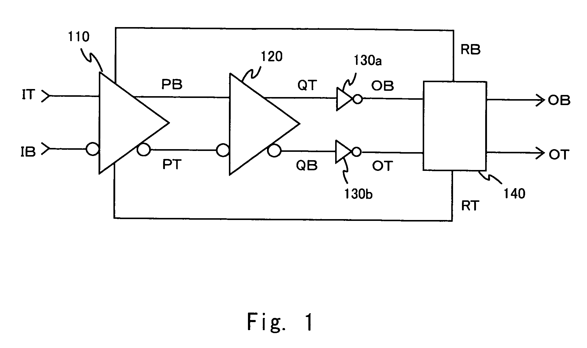
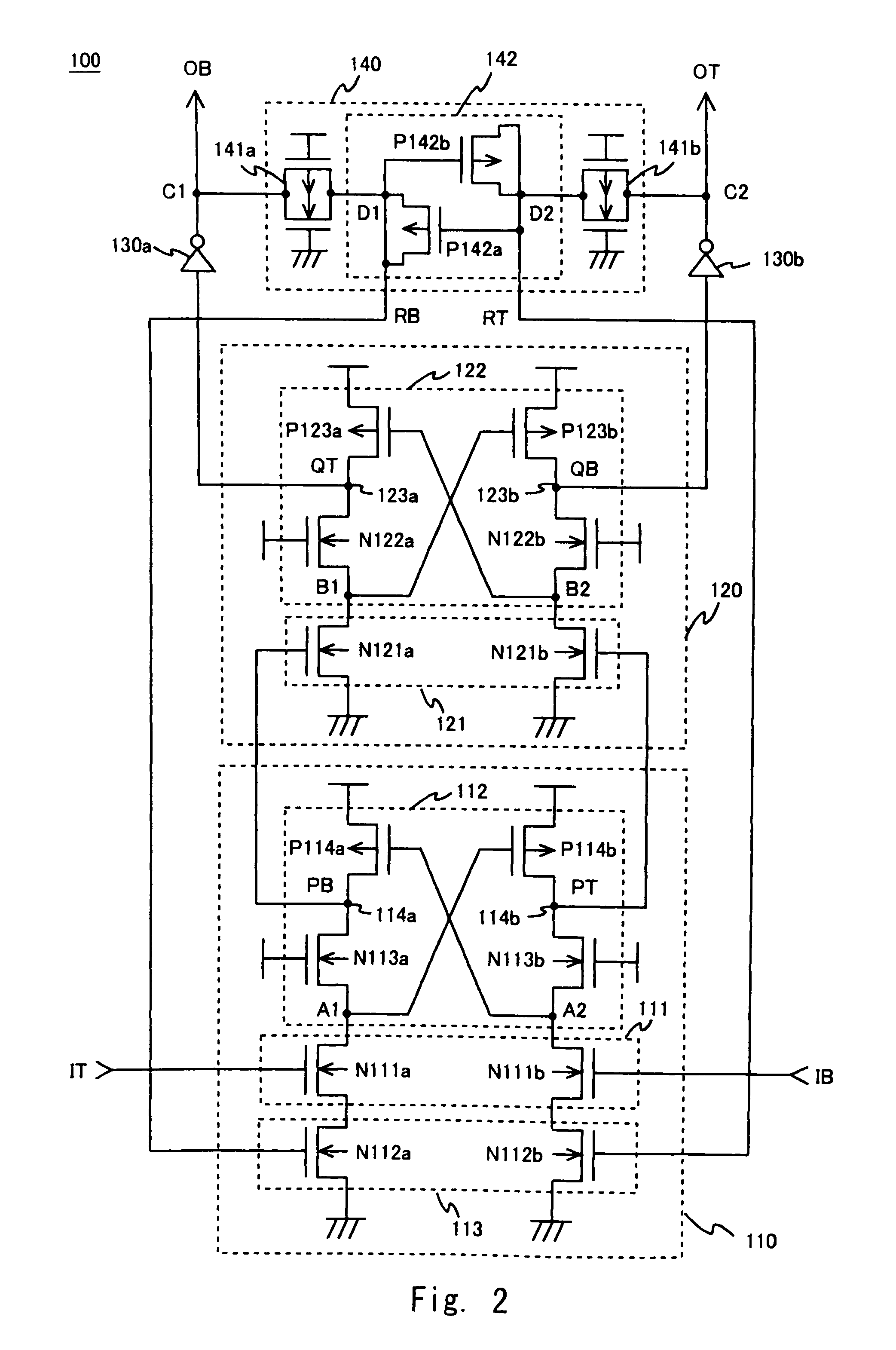
[0013]The semiconductor circuit according to the present invention feeds back a DC voltage component of an offset from the differential signal output terminals, which is extracted from the low-pass filter, to the differential input section receiving the input differential signal. A feedback loop is constituted so that the DC voltage component fed back as described above is used by the load adjustment section to adjust the resistance value of the load resistance section. Accordingly, the circuit constituting the feedback loop corrects the degradation in duty cycle of the differential signals output from the differential signal output terminals.
[0014]According to the present invention, it is possible to correct not only the degradation in duty cycle of input differential signals, but also the degradation in duty cycle due to variations among transistors constituting the circuit itself, which cannot be corrected by the conventional differential amplifier, with a simple circuit configuration.

Problems solved by technology

In the differential amplifier 1900 as shown in FIG. 19, when the differential signals IT / IB to be input have different offsets, there arises a problem in that offset components are also amplified, with the result that the degradation in duty cycle is increased.
In other words, it is impossible to prevent the degradation in duty cycle of the output differential clock signals due to relative process variations among transistors constituting the differential amplifier 2000 itself, imbalance in parasitic capacitance and parasitic resistance of wires of the differential amplifier 2000, and the like.
Further, it is impossible to obtain the effect of correcting the degradation in duty cycle of the differential signals caused by relative variations among transistors constituting the differential amplifier 2000 and subsequent circuits.
In the technique, however, if elements such as transistors constituting a correction differential amplifier vary, there arises a problem in that an input offset cannot be compensated and the duty cycle of a differential signal to be output is degraded.

Method used


Image

  • Semiconductor circuit
  • Semiconductor circuit
  • Semiconductor circuit

Examples


first embodiment

[0040]Hereinafter, a specific first embodiment of a semiconductor circuit to which the present invention is applied will be described in detail with reference to the drawings. In the first embodiment, the present invention is applied to a semiconductor circuit 100 to amplify small-amplitude differential clock signals and convert the amplified differential clock signals into large-amplitude differential clock signals.

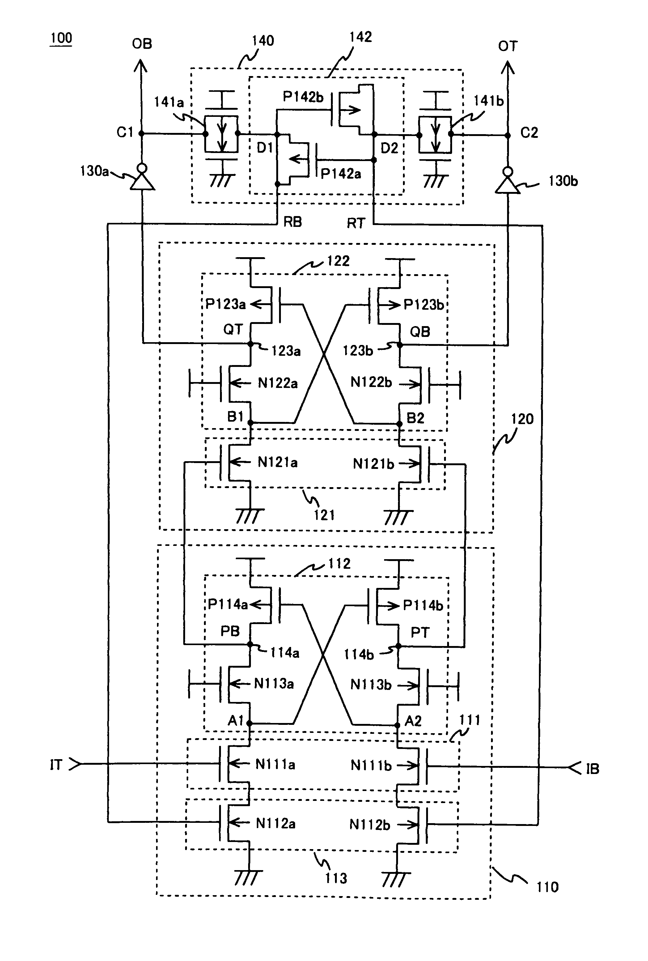
[0041]FIG. 1 shows an example of a schematic configuration of the semiconductor circuit 100 according to the first embodiment. The semiconductor circuit 100 includes differential amplifiers 110 and 120, CMOS inverters 130a and 130b, and a low-pass filter 140. The differential amplifier 110 receives input differential signals IT / IB and outputs amplified differential signals PB / PT. The differential amplifier 120 receives the differential signals PB / PT and outputs amplified differential signals QT / QB. The CMOS inverters 130a and 130b invert the differential signals QT / QB, r...


PUM


Abstract

A semiconductor circuit according to the present invention includes: a differential input section to receive input differential signals; a load resistance section to output a voltage according to a current output by the differential input section; differential signal output terminals to output a differential signal corresponding to the voltage output from the load resistance section; a low-pass filter to extract a direct-current component of the differential signal output from the differential signal output terminals; and a load adjustment section to feed back the direct-current component extracted by the low-pass filter to adjust a resistance value of the load resistance section.

Description

BACKGROUND OF THE INVENTION[0001]1. Field of the Invention[0002]The present invention relates to a semiconductor circuit and, more particularly, to a semiconductor circuit to correct degradation in duty cycle of a differential signal to be output.[0003]2. Description of Related Art[0004]In recent years, current mode logic (CML) has been attracting much attention as a high-speed signal transmission system. In the CML, a differential signal transmission system is employed to transmit signals. Moreover, in the CML, a signal level having a small amplitude (hereinafter, referred to as “CML level”) is used, and in an internal circuit to which signals are transmitted, a signal level having a large amplitude (hereinafter, referred to as “CMOS level”) in a range from a power supply voltage to a ground voltage is used.[0005]FIG. 18 shows a schematic diagram of a circuit 1800 receiving differential clock signals that are small signals such as the CML level, to convert the differential clock si...

Claims


Application Information

Patent Timeline
Patent Type & Authority Patents(United States)
IPC IPC(8): H03K3/017
CPCH03K3/35613G11C7/22H03F3/45H03K3/2885H03K19/0175
Inventor AOKI, YASUSHI
Owner RENESAS ELECTRONICS CORP
Learn More