Semiconductor device for latch-up prevention

Active Publication Date: 2010-08-17
MICROSEMI STORAGE SOLUTIONS
View PDF14 Cites 15 Cited by
  • Summary
  • Abstract
  • Description
  • Claims
  • Application Information

AI Technical Summary

Benefits of technology

[0017]It is an object of the present invention to improve the performance of latch-up prevention devices while reducing their size, which provides for more robust and cost effective devices.
[0027]The first implanted region forms a first parasitic bipolar transistor dominantly of the first connectivity type with the first well and the second well, and the fifth implanted region forming a second parasitic bipolar transistor dominantly of the second connectivity type with the first well and the third well. The natively doped region creates a separation resistance that helps the current received upon activation of the first parasitic bipolar transistor to flow through the third implanted region of the second well away from the second parasitic bipolar transistor in order to avoid latch up.

Problems solved by technology

However, cycling the power supply causes down-time and needs to be done manually unless latch-up detection circuitry is being used.
If the short-circuit current that flows through the SCR is large, physical damage to circuitry may also occur due to the heat generated.
Furthermore, a parasitic SCR that is near an injector is at risk of entering latch-up.
Since such options may increase the cost of fabrication or may simply not be available, these methods are not always practical.
Furthermore, as the current technology aims to reduce the size of integrated circuit chips, the area consumed by guard rings and space regions affects the overall cost of producing the chip.

Method used


Image

  • Semiconductor device for latch-up prevention
  • Semiconductor device for latch-up prevention
  • Semiconductor device for latch-up prevention

Examples


Embodiment Construction

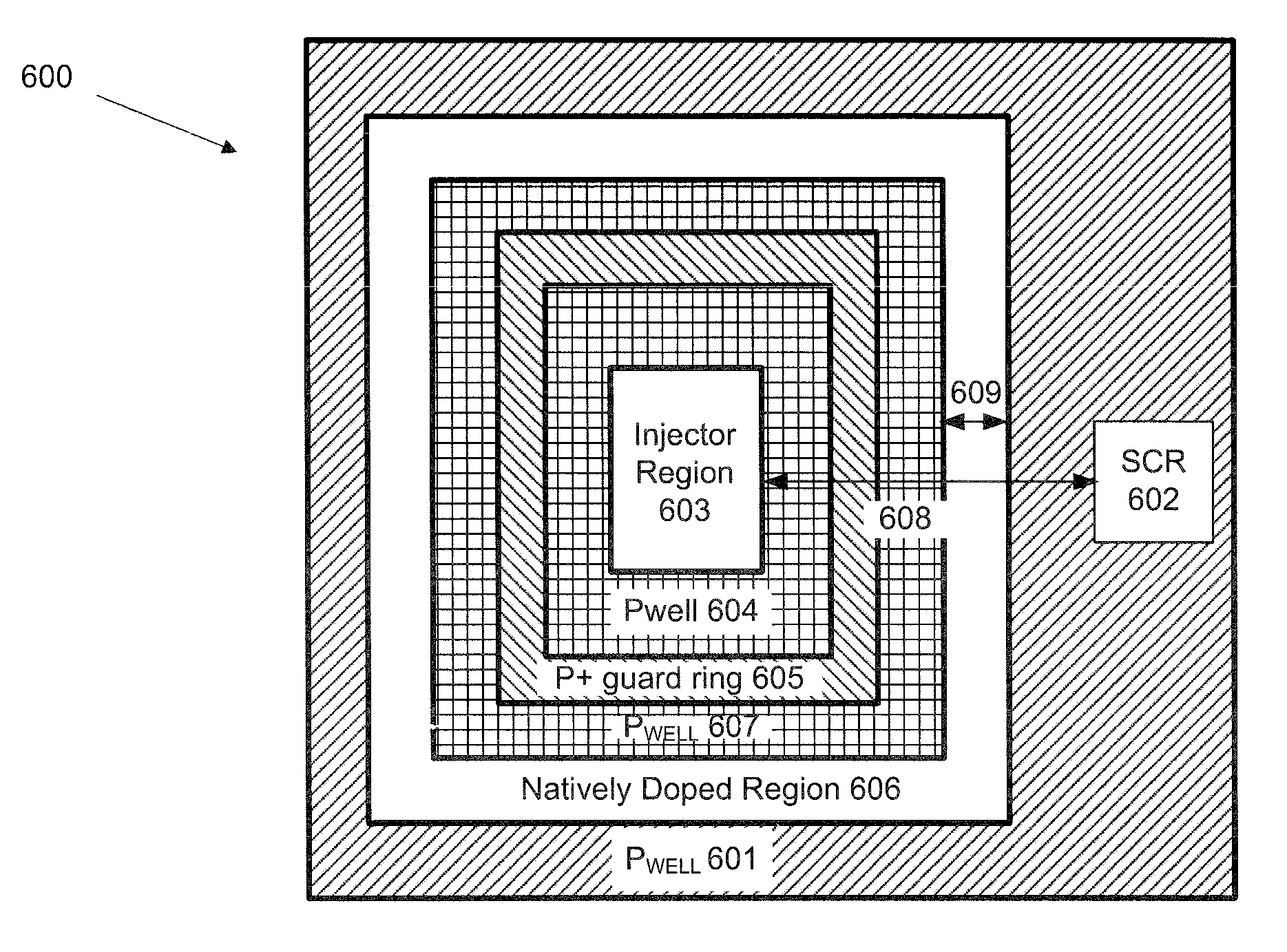
[0051]Generally, the present invention provides a method and system for improving the efficiency of semiconductor devices that prevent latch-up in SCRs, by providing more efficient guard rings and spacing without increasing the size of the latch-up prevention device.

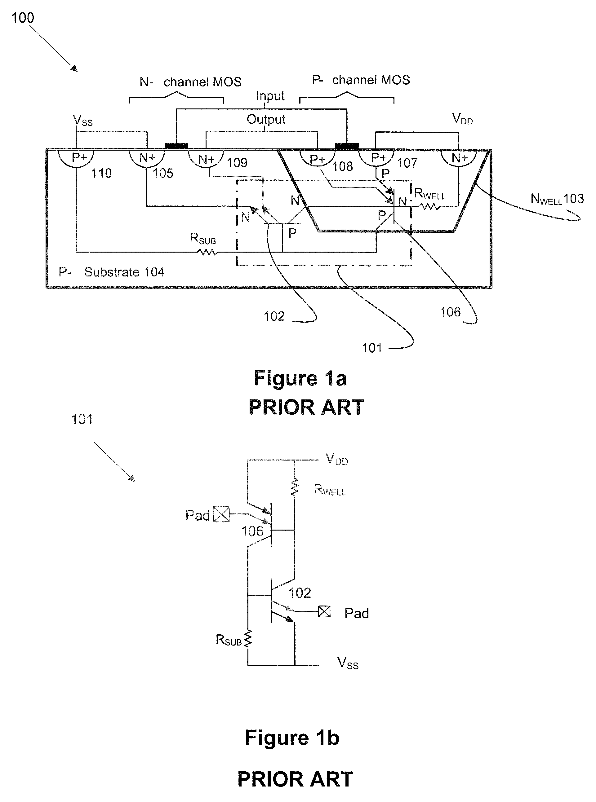
[0052]Embodiments of the invention provide a semiconductor device for preventing latch-up in SCRs when these SCRs become activated. A natively doped region having high resistance is used to separate an NPN transistor from a PNP transistor in the SCR, and / or to isolate the entire SCR from the injector source in order to prevent latch-up. The high resistance of the natively doped region allows the device to achieve the separation resistance needed in a smaller space, as compared to the space required to achieve the same separation resistance in a well. Accordingly, more robust and cost effective latch-up prevention devices are provided.

[0053]In order to decrease the area of the latch-up prevention device, embodiments of th...


PUM


Abstract

A semiconductor device is provided for preventing Latch-up in Silicon Controlled Rectifiers (SCRs) when these SCRs become activated. Embodiments of the invention use a natively doped region having high resistance to separate the NPN transistor from the PNP transistor that form the SCR, and / or to isolate the entire SCR from the injector source in order to prevent latch-up. The high resistance of the natively doped region allows to achieve the separation resistance needed in a smaller space, as compared to the space required to achieve the same separation resistance in a well. Accordingly, the invention provides for more robust and cost effective latch-up prevention devices.

Description

CROSS REFERENCE TO RELATED APPLICATIONS[0001]This application is related to U.S. patent application Ser. No. 12 / 242,225 filed on Sep. 30, 2008, and entitled “A SEMICONDUCTOR DEVICE FOR ELECTROSTATIC DISCHARGE PROTECTION” which is incorporated herein by reference in its entirety.FIELD OF THE INVENTION[0002]The present invention relates generally to semiconductor devices. More particularly, the present invention relates to semiconductor devices for latch-up prevention.BACKGROUND OF THE INVENTION[0003]Parasitic bipolar transistors of CMOS circuits can form Silicon Controlled Rectifiers (hereinafter referred to as SCRs). An SCR typically includes two parasitic bipolar transistors that are dominantly of opposite connectivity types, such as an NPN parasitic bipolar transistor (hereinafter referred to as NPN) and a PNP parasitic bipolar transistor (hereinafter referred to as PNP). Since the NPN has two junctions of N and one junction of P it is considered to be dominantly an N-type transis...

Claims


Application Information

Patent Timeline
IPC IPC(8): H01L29/74
CPCH01L29/0692H01L29/7436
Inventor BOYD, GRAEME B.CHENG, XUNSIBLEY, ARIEL D. E.
Owner MICROSEMI STORAGE SOLUTIONS
Why Eureka
Try Eureka