

Normally-off field-effect semiconductor device
a field-effect semiconductor and field-effect technology, applied in the field of field-effect semiconductor devices, can solve the problems of reducing the electron concentration in the two-dimensional electron gas layer, and unnecessary complex and expensive associated electric circuitry, so as to reduce the gate leak current, reduce the resistance, and eliminate the effect of fluctuations from one device to another
- Summary
- Abstract
- Description
- Claims
- Application Information
AI Technical Summary
Benefits of technology
Problems solved by technology
Method used
Image

Examples
embodiment
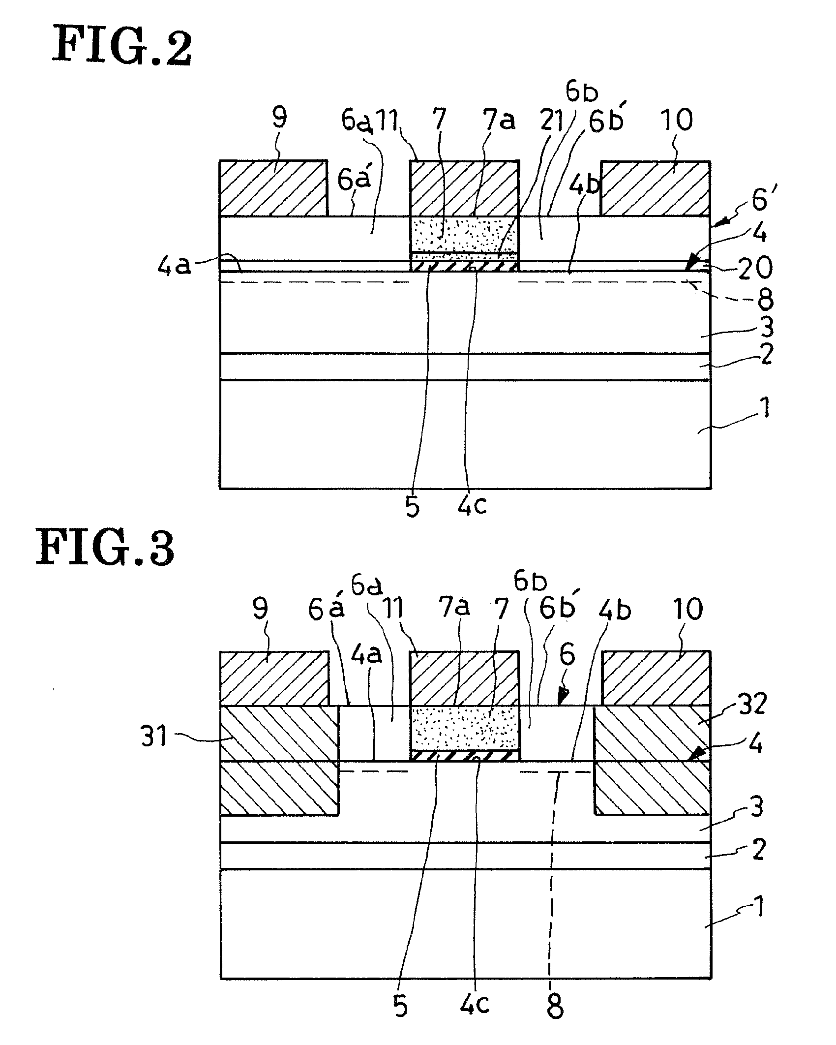
of FIG. 2
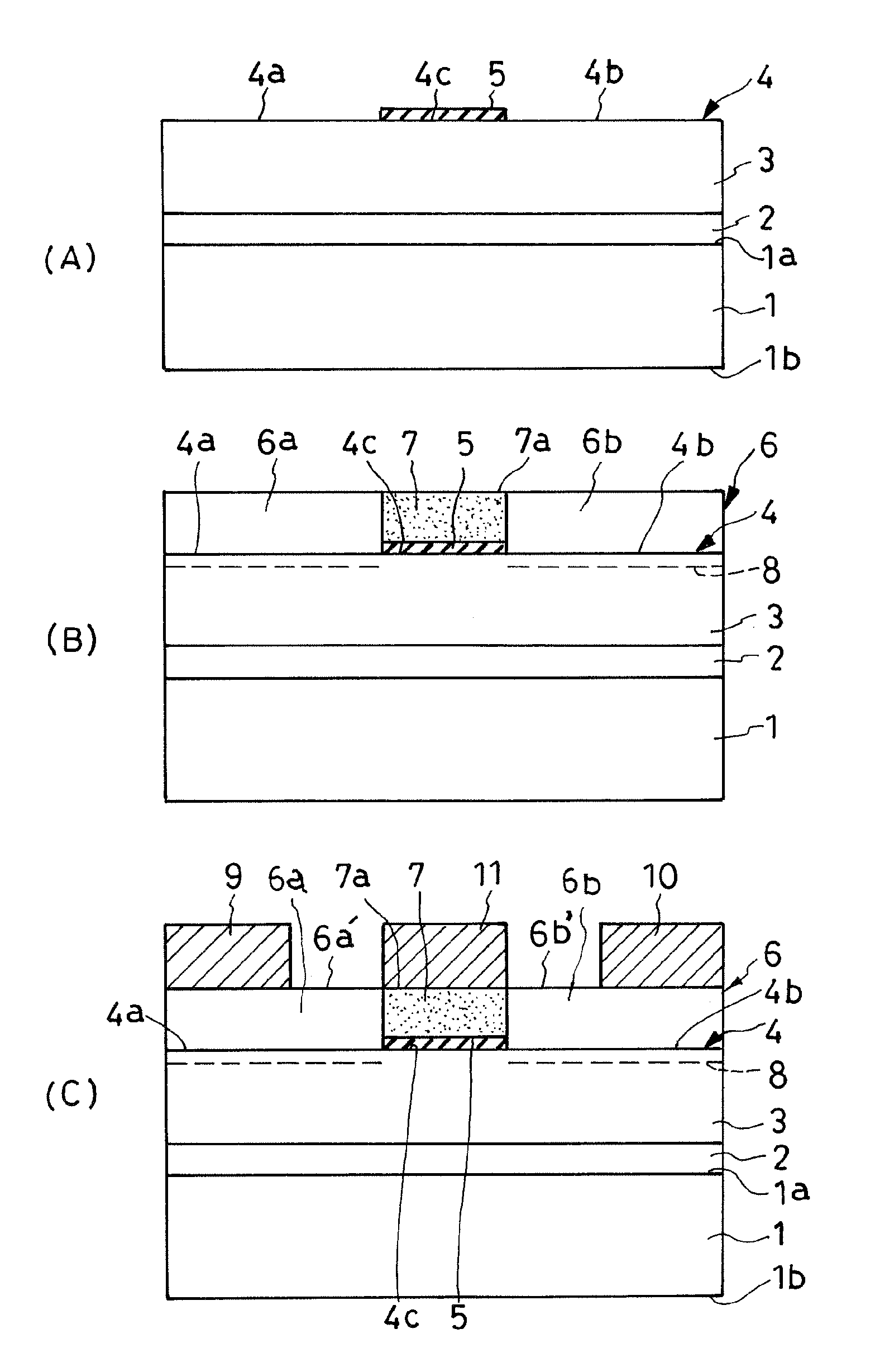
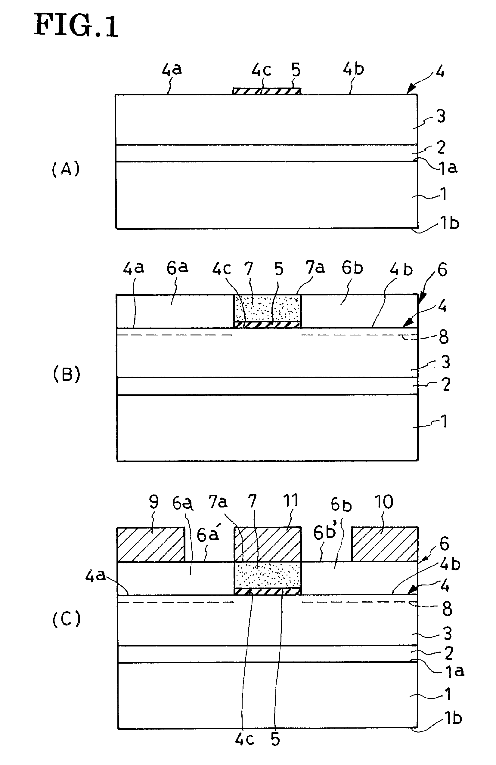
[0047]The second preferred form of HEMT-like field-effect semiconductor device features a modified two-part electron supply layer 6′ and a spacer 20 between the electron transit layer 3 and the modified electron supply layer 6′. All the other details of construction are substantially as set forth above with reference to FIG. 1.
[0048]The modified two-part electron supply layer 6′ together with the discontinuous growth layer 7 is made from any of the n-doped semiconducting nitrides that are generally defined by the formula:
AlaGa1-aN
where the subscript a is a numeral that is greater than zero and less than one, greater than a in the formula above defining the materials for the electron transit layer 3, preferably in the range of 0.2 through 0.4, and most desirably 0.3; or by the formula:
AlaInbGa1-a-bN
where the subscript a is a numeral that is greater than zero and less than one, and greater than a in the formula above defining the materials for the electron transit layer 3; th...
PUM
 Abstract
Description
Claims
Application Information