Differential circuit providing a function to cancel input offset voltage

a differential circuit and offset voltage technology, applied in differential amplifiers, amplifier details, amplifiers with semiconductor devices/discharge tubes, etc., can solve the problems of reducing the signal quality in the lower frequencies, affecting the gain of the inverting amplifier and the capacitance obtained, and raising the cost of the i

Active Publication Date: 2010-08-24
SUMITOMO ELECTRIC IND LTD
View PDF4 Cites 4 Cited by
  • Summary
  • Abstract
  • Description
  • Claims
  • Application Information

AI Technical Summary

Benefits of technology

[0008]The Miller amplifier of the invention may include a differential amplifier and resistors each connected with the differential amplifier so as to constitute an inverting amplifier. The closed loop gain of this inverting amplifier is solely determined by the resistance ratio of these resistors; thus, the gain may be free from the input level of the inverting amplifier. The differential amplifier may be a general purpose operational amplifier easily available in the market.

Problems solved by technology

Because of its large capacitance, the capacitor in the low-pass filter or the integrator often configures as an external capacitor, which inevitably forces the IC to provide additional two lead pins for the external capacitor.
When the capacitor for the low-pass filter or the integrator is set within the IC, the die area must be enlarged, which raises the cost of the IC.
However, this circuit varies the trans-conductance gm of the transistor depending on the gate bias, which also changes the gain of the inverting amplifier and the capacitance obtained by the Miller effect.
Applying this offset canceller to the differential circuit for the optical communication system, the instability of the input bias due to a change of the ambient and operational temperature and a drift of the power supply or the input signal with relatively low frequency components change the Miller capacitance of the inverting amplifier, which makes the cut-off frequency of the filter or the integrator instable; thus the signal quality in the lower frequencies is degraded.

Method used


Image

  • Differential circuit providing a function to cancel input offset voltage
  • Differential circuit providing a function to cancel input offset voltage
  • Differential circuit providing a function to cancel input offset voltage

Examples


first embodiment

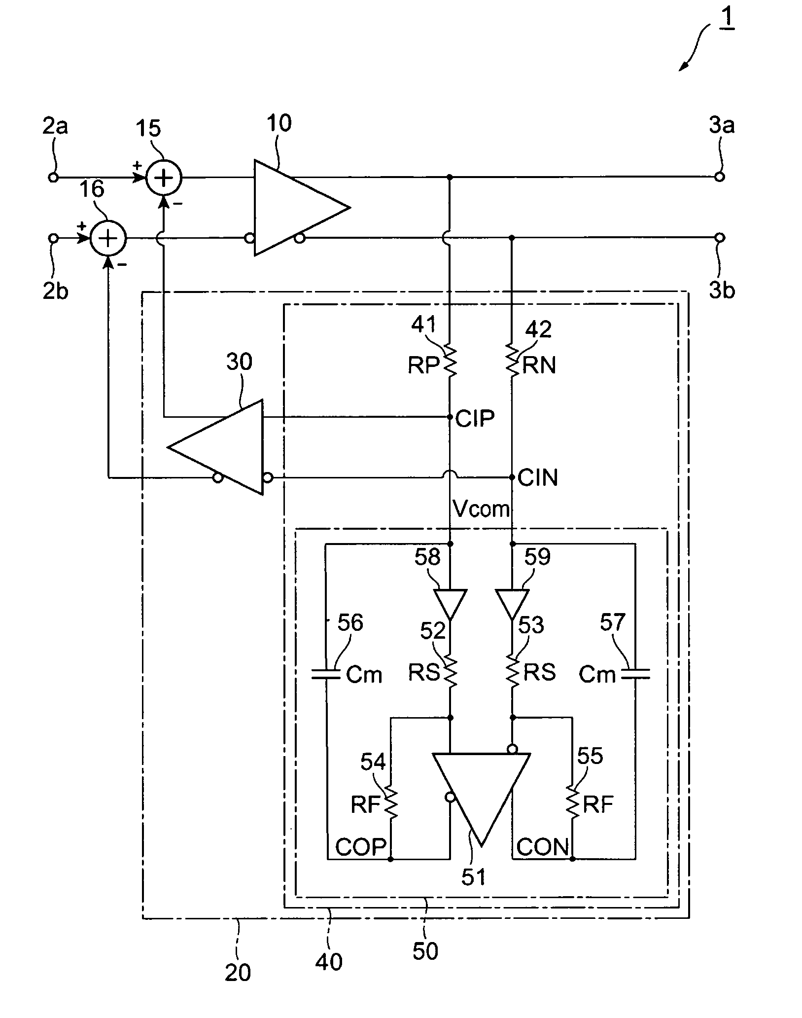
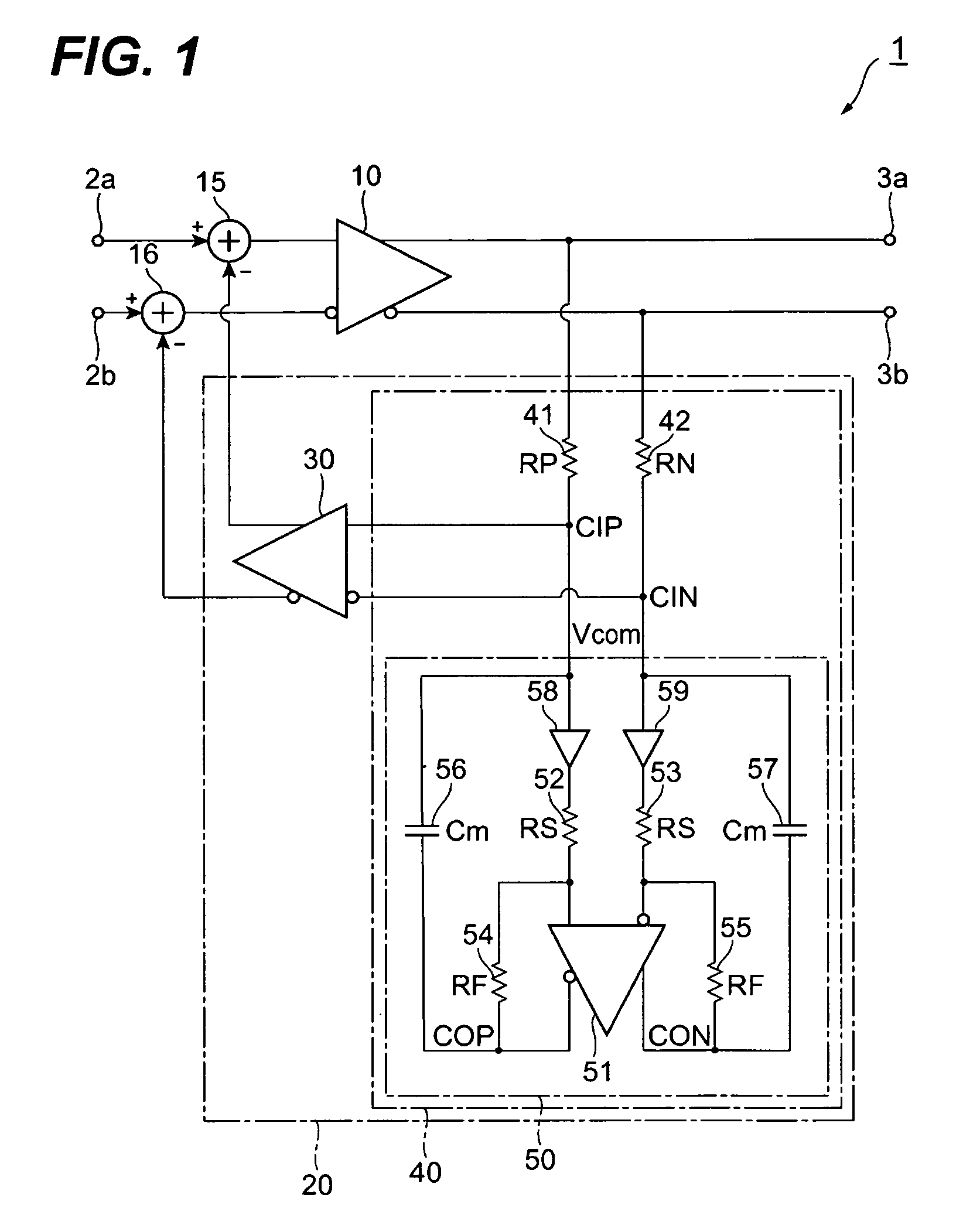
[0022]FIG. 1 illustrates a circuit diagram of a differential circuit and an offset canceller according to the first embodiment of the invention. The 1 provides a pair of input terminals, 2a and 2b, a pair of output terminals, 3a and 3b, a primary amplifier 10, an offset canceller 20 and two subtractors, 15 and 16.

[0023]The primary amplifier 10, put between two input terminals, 2a and 2b, and two output terminals, 3a and 3b, is connected in the non-inverting input thereof with the input terminal 2a through the 15, while, in the inverting input thereof is coupled with the input terminal 2b through the other 16. The non-inverting output of the primary amplifier 10 is directly coupled with the output terminal 3a, while, the inverting output thereof is coupled with the other output terminal 3b. Here, the inverting and the non-inverting merely mean that the signals output therefrom or input thereto have phases opposite to each other.

[0024]The primary amplifier 10 typically comprises a plu...

second embodiment

[0051]FIG. 4 is a circuit diagram of a differential circuit according to the second embodiment of the present invention. The differential circuit 1A has a different feature from those of the first embodiment shown in FIG. 1 that the differential circuit 1A provides, instead of the offset canceller 20, a modified offset canceller 20A. Other arrangements except for the offset canceller 20A are same with those in the first circuit 1. The offset canceller 20A may be distinguished from the aforementioned offset canceller 20 by the filter 40A. The filter 40A provides a trans-conductance amplifier 43 but removes the first and second resistors, 41 and 42.

[0052]The trans-conductance amplifier 43 converts a voltage signal into a current signal. Accordingly, the trans-conductance amplifier 43 may be regarded as a conductive element whose conductance is the inverse of the resistance of a resistor. Because the trans-conductance amplifier 43 has the converting gain, gm [A / V], the filter 40A provi...

third embodiment

[0057]FIG. 7 shows another modified differential circuit according to the third embodiment of the invention. The third differential circuit 1B has a feature to provide another offset canceller 20B instead of the aforementioned offset canceller 20. Other configurations of the third differential circuit 1B are same with those of the first 1.

[0058]The offset canceller 20B provides, in place of the capacitance multiplier 50, a modified capacitance multiplier SOB that includes an Op-Amp 51B. This Op-Amp 51B provides a function to adjust the output level responding to the control signal VCM. The output level of the Op-Amp 51B is desirable to be set in a middle level within an output swing range of the Op-Amp 51B. Other functions of the Op-Amp 51B are same with those of the former Op-Amp 51.

[0059]When the closed loop gain of the Op-Amp 51 combined with the resistors, 52 to 55, is large, the capacitance multiplier 50 occasionally causes the saturation in the output level thereof depending o...


PUM


Abstract

A new offset canceling circuit for a differential circuit is disclosed whose input offset voltage may be cancelled independent of the variation of the input level, accordingly, enables the cut-off frequency of the canceling circuit unchanged. The offset canceller of the invention provides a buffer amplifier and a filter. The filter includes a capacitance multiplier including an operational amplifier (Op-Amp) operating in the inverting mode and a capacitor connected between the input and output of the Op-Amp. The Op-Amp operating in the inverting mode whose closed loop gain is solely determined by resistors, and the capacitance of the capacitor is multiplied by the closed loop gain of the Op-Amp by the Miller effect.

Description

BACKGROUND OF THE INVENTION[0001]1. Field of the Invention[0002]The present invention relates to a circuit to cancel a DC offset appeared in a differential circuit, and a differential circuit providing this offset canceller.[0003]2. Related Prior Art[0004]A differential circuit, especially a circuit applied in an optical communication system, is necessary to amplify a signal with a broadband width from low frequencies, typically 1 kHz, to high frequencies, typically 1 MHz. Such a differential circuit usually provides a DC offset canceller including a low-pass filter or an integrator accompanied with a capacitor. Because of its large capacitance, the capacitor in the low-pass filter or the integrator often configures as an external capacitor, which inevitably forces the IC to provide additional two lead pins for the external capacitor. When the capacitor for the low-pass filter or the integrator is set within the IC, the die area must be enlarged, which raises the cost of the IC.[000...

Claims


Application Information

Patent Timeline
Patent Type & Authority Patents(United States)
IPC IPC(8): H03F3/45
CPCH03F3/45183H03F3/45475H03F3/45748H03F3/45973H03F2203/45138H03F2203/45212H03F2203/45441H03F2203/45521H03F2203/45588H03F2203/45682
Inventor TANAKA, KEIJI
Owner SUMITOMO ELECTRIC IND LTD
Why Eureka
Try Eureka