Buried semiconductor laser and method for manufacturing the same

a semiconductor laser and buried technology, applied in semiconductor lasers, laser details, electrical devices, etc., can solve the problems of deteriorating laser characteristics, adversely affecting the reliability of the semiconductor device, and devices that are structurally vulnerable, so as to reduce the dislocation of the contact layer

Inactive Publication Date: 2010-08-24
RENESAS ELECTRONICS CORP
View PDF5 Cites 0 Cited by
  • Summary
  • Abstract
  • Description
  • Claims
  • Application Information

AI Technical Summary

Benefits of technology

[0013]According to one aspect of the present invention, there is provided a buried semiconductor laser, comprising: an n-type indium phosphide (InP) substrate; an active layer disposed on the n-type InP substrate; block layers bilaterally provided on both sides of the active layer; a clad layer provided over the active layer and the block layers; and a p-type gallium indium arsenide (InGaAs) contact layer provided over the clad layer, wherein the p-type InGaAs contact layer has a compressive strain. A strain to be applied to the contact layer can be suitably controlled to reduce a tensile strain in the whole contact layer, so that a contact layer, which exhibits reduced chances of a generation of a dislocation, can be obtained.
[0016]A composition of the flat portion is corrected toward a side of the compressive strain in the growth of the layer, so that the tensile strain in the inclined portion is reduced, thereby avoiding a generation of a defect such as dislocation and the like.
[0018]A p-type InGaAs contact layer having a thickness of 0.3 μm, which is a sufficient thickness for ensuring a diffusion length after an alloy process with an electrode metal, which is a necessary process for providing better ohmic contact with the electrode metal, was employed to conduct an investigation for a critical strain level on the basis of a model proposed by J. W. Matthews and A. E. Blakeslee (J. Crystal Growth, 27 (1974), J. W. Matthews and A. E. Blakeslee, 118-125), and the results of the investigation show that the compressive strain in the flat portion within a range of from 0.1% to 0.2% would provides a formation of the p-type InGaAs contact layer having the flat portion and the inclined portion, each of which has a thickness that is not higher than a critical strain, thereby reducing a generation of a defect such as dislocation and the like. The thickness of the p-type InGaAs contact layer of equal to or smaller than 0.3 μm provides further larger tolerance for the compressive strain composition of the p-type InGaAs contact layer.
[0021]According to the present invention, the buried semiconductor laser exhibiting a reduced dislocation of the contact layer is achieved.

Problems solved by technology

However, when a strain larger than a critical strain is applied to a quantum well layer, a defect such as dislocation is generated in an emission layer, considerably deteriorating laser characteristics.
Since a larger strain to the active layer is applied to the semiconductor devices described above at a level up to the limit of the material property, the devices are structurally vulnerable by a stress generated in the whole laser device.
Such tensile strain generated at the inclined portion of the p-type InGaAs contact layer immediately above the active layer may possibly induce a generation of a defect such as dislocation and the like, causing a concern for adversely affecting a reliability of the semiconductor device.
In general, the atomic uptake efficiency between the inclined portion and the flat portion is varied somewhat by growth conditions of the p-type InGaAs layer, but it is difficult to obtain the same composition for the inclined portion and for the flat portion.
A tensile strain in the portion of the p-type InGaAs contact layer in the inclined portion immediately above the active layer may induce a generation of a defect such as dislocation and the like, leading to adversely affecting a reliability of the semiconductor device.

Method used


Image

  • Buried semiconductor laser and method for manufacturing the same
  • Buried semiconductor laser and method for manufacturing the same
  • Buried semiconductor laser and method for manufacturing the same

Examples


first embodiment

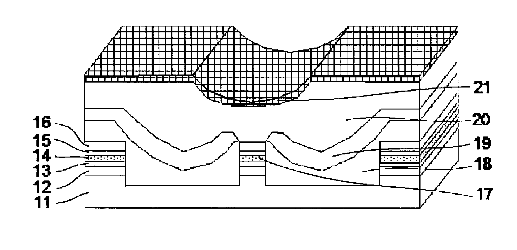
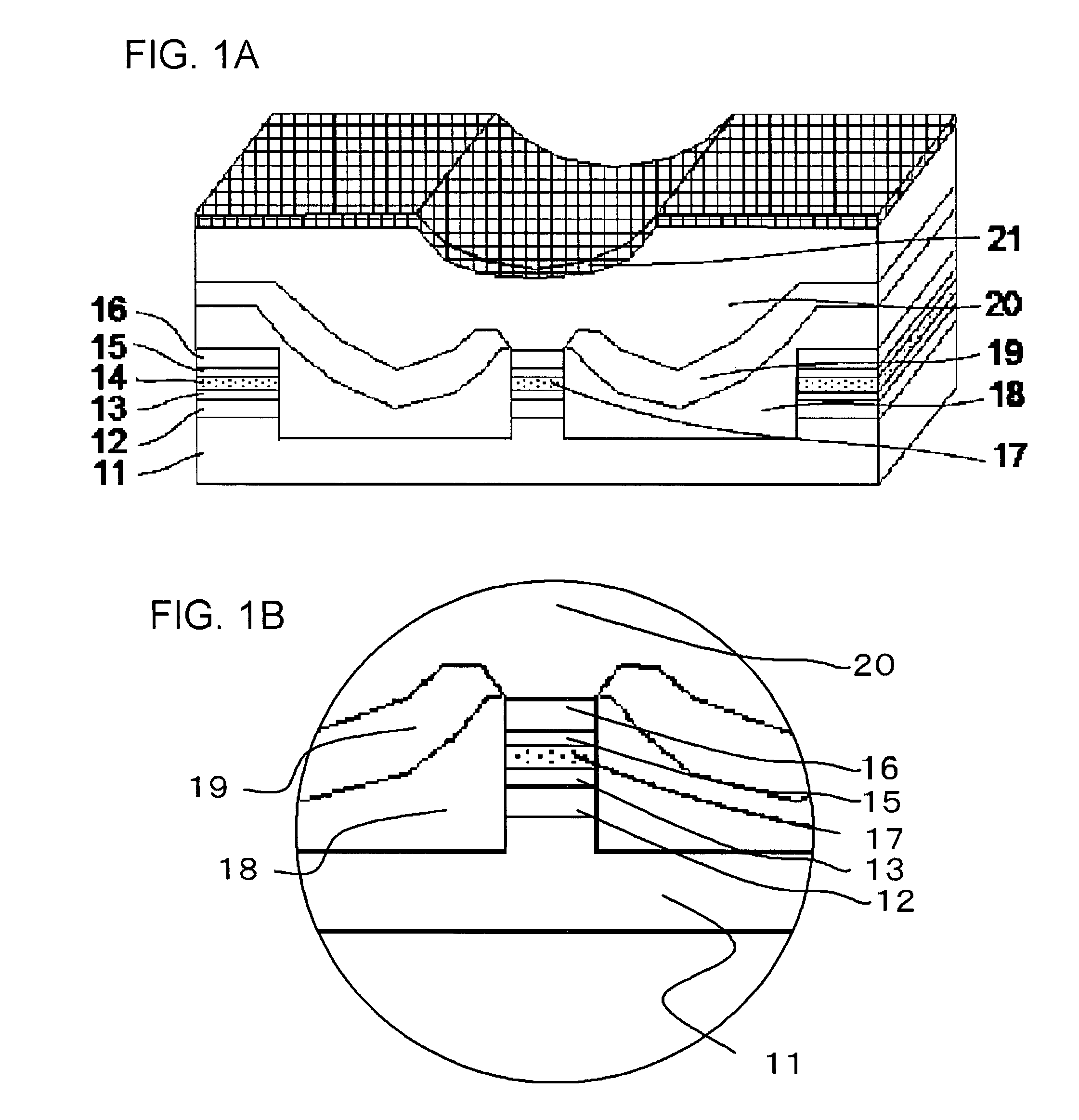
[0033]FIG. 1A illustrates a structure of a buried semiconductor laser according to the first embodiment of the present invention. The semiconductor device of the present embodiment includes an n-type InP substrate 11, an active layer 17 as a light emitting region, a p-type current block layer 18, an n-type current block layer 19, a p-type clad layer 20, and a p-type InGaAs contact layer 21.

[0034]The block layers 18 and 19 are provided on both sides of the active layer 17. In other words, the active layer 17 is disposed between a pair of the block layers 18 and 19. The p-type clad layer 20 is disposed so as to cover the active layer 17 and the block layers 18 and 19.

[0035]FIG. 1B illustrates an enlarged view of a structure around the active layer 17 showed in FIG. 1A. A mesa structure including an n-type InP clad layer 12, n-side InGaAsP guide layer 13, the active layer 17, a p-side InGaAsP guide layer 15, and a p-type InP clad layer 16 is provided on the n-type InP substrate 11. The...

second embodiment

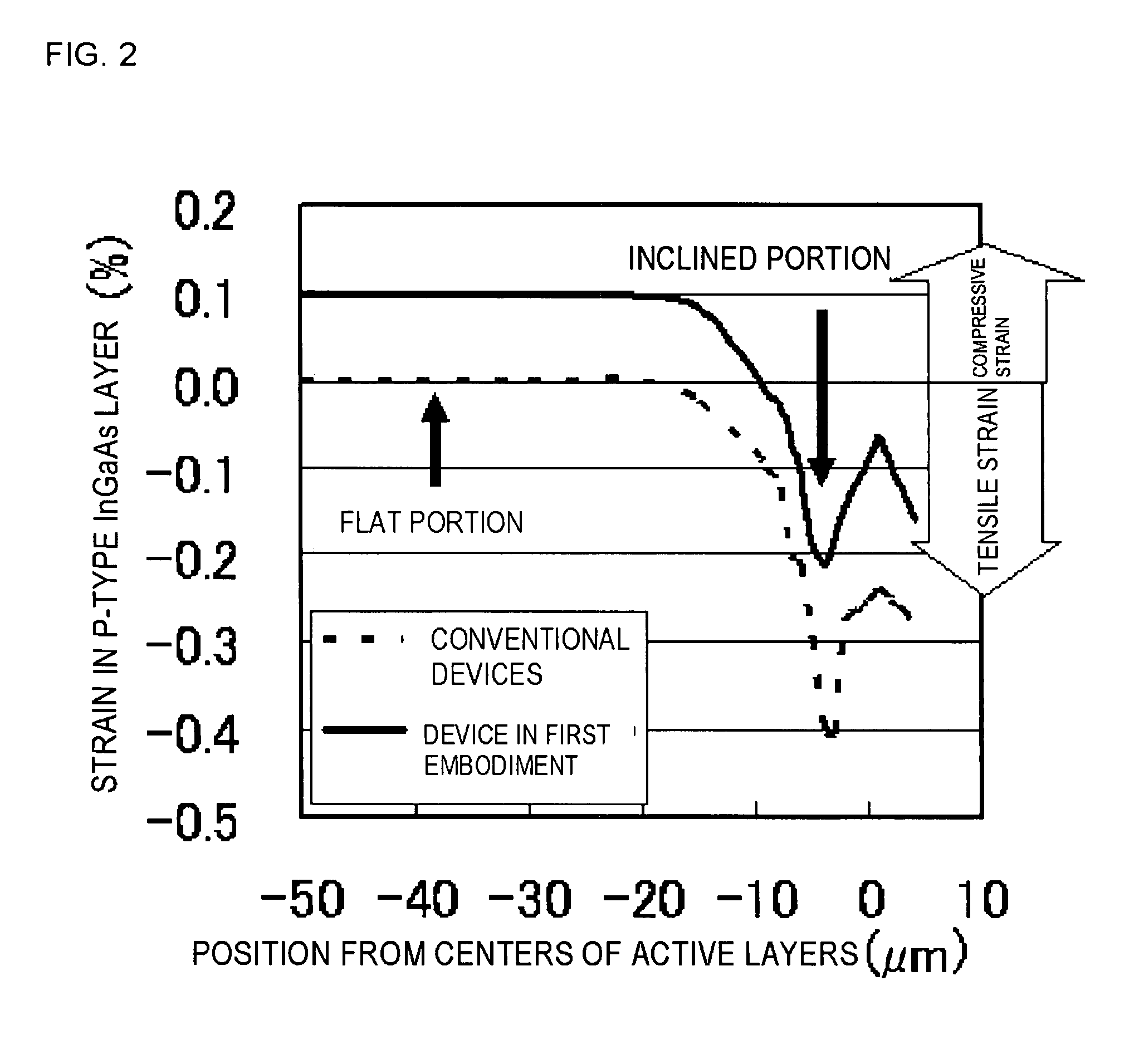
[0046]In reference to FIG. 3, another embodiment of a buried semiconductor laser, in which the p-type InGaAs contact layer 21 in FIG. 1 is replaced with a superlattice structure of a p-type InAs layer and a p-type GaAs layer will be described. In FIG. 3, the p-type InGaAs contact layer 31 is composed of a superlattice structure of a p-type InAs layer 32 and a p-type GaAs layer 33. In the present embodiment, similarly as in first embodiment, a growth is conducted to reach the p-type InP clad layer 20, and then an InAs / GaAs superlattice structure 31 composed of the p-type InAs layer 32 and the p-type GaAs layer 33 is grown. In such case, it is confirmed that the p-type InAs / GaAs superlattice structure 31 is grown to have an average compressive strain within a range of from 0.1% to 0.2% in the flat portion thereof that is sufficiently remote by 50 μm or further from the portion thereof immediately above the active layers, so that the flat portion and the inclined portion immediately ab...


PUM


Abstract

A buried semiconductor laser exhibiting a reduced dislocation of a contact layer is achieved. A buried semiconductor laser, comprising: an n-type indium phosphide (InP) substrate; an active layer disposed on the n-type InP substrate; block layers provided so as to bilaterally disposed on both sides of the active layer; a clad layer provided so as to cover the active layer and the block layers; and a p-type gallium indium arsenide (InGaAs) contact layer provided on the clad layer, wherein the p-type InGaAs contact layer has a compressive strain.

Description

[0001]This application is based on Japanese patent application No. 2006-333,261, the content of which is incorporated hereinto by reference.BACKGROUND[0002]1. Technical Field[0003]The present invention relates to a buried semiconductor laser and a method for manufacturing the same. Specifically, the present invention relates to a structure of a p-type gallium indium arsenide (InGaAs) contact layer in a buried semiconductor laser of group III-V element, employed for optical communications, and a method for manufacturing the same.[0004]2. Related Art[0005]In an optical transmission system that achieves a communication with higher capacity and higher rate, semiconductor lasers employed as light sources are mainly composed of indium phosphide (InP)-containing, group III-V compound semiconductors. Lower threshold current and higher efficiency are required for an active layer in a semiconductor laser, so that a strained quantum-well structure is used in order to improve such characteristi...

Claims


Application Information

Patent Timeline
Patent Type & Authority Patents(United States)
IPC IPC(8): H01S5/00H01S5/227H01S5/343
CPCB82Y20/00H01S5/227H01S5/0425H01S5/2201H01S5/2206H01S5/2226H01S5/2275H01S5/305H01S5/3054H01S5/3201H01S5/34306H01S5/04254
Inventor AE, SATOSHI
Owner RENESAS ELECTRONICS CORP
Why Eureka
Try Eureka