Multiphase clock for superconducting electronics

a superconducting electronics and multi-phase clock technology, applied in the direction of instruments, pulse techniques, generating/distributing signals, etc., to achieve the effect of improving long-term performan

Inactive Publication Date: 2010-08-31
HYPRES
View PDF6 Cites 25 Cited by
  • Summary
  • Abstract
  • Description
  • Claims
  • Application Information

AI Technical Summary

Benefits of technology

[0016]The multiphase clock signals may be applied to a digital I-Q mixer circuit, leading to improved long-term performance.

Problems solved by technology

Because the DFFs are destructive memory cells that are reset every period, they retain no memory and hence rare errors are clocked out during each clock cycle; they do not accumulate or re-circulate.

Method used


Image

  • Multiphase clock for superconducting electronics
  • Multiphase clock for superconducting electronics
  • Multiphase clock for superconducting electronics

Examples


Embodiment Construction

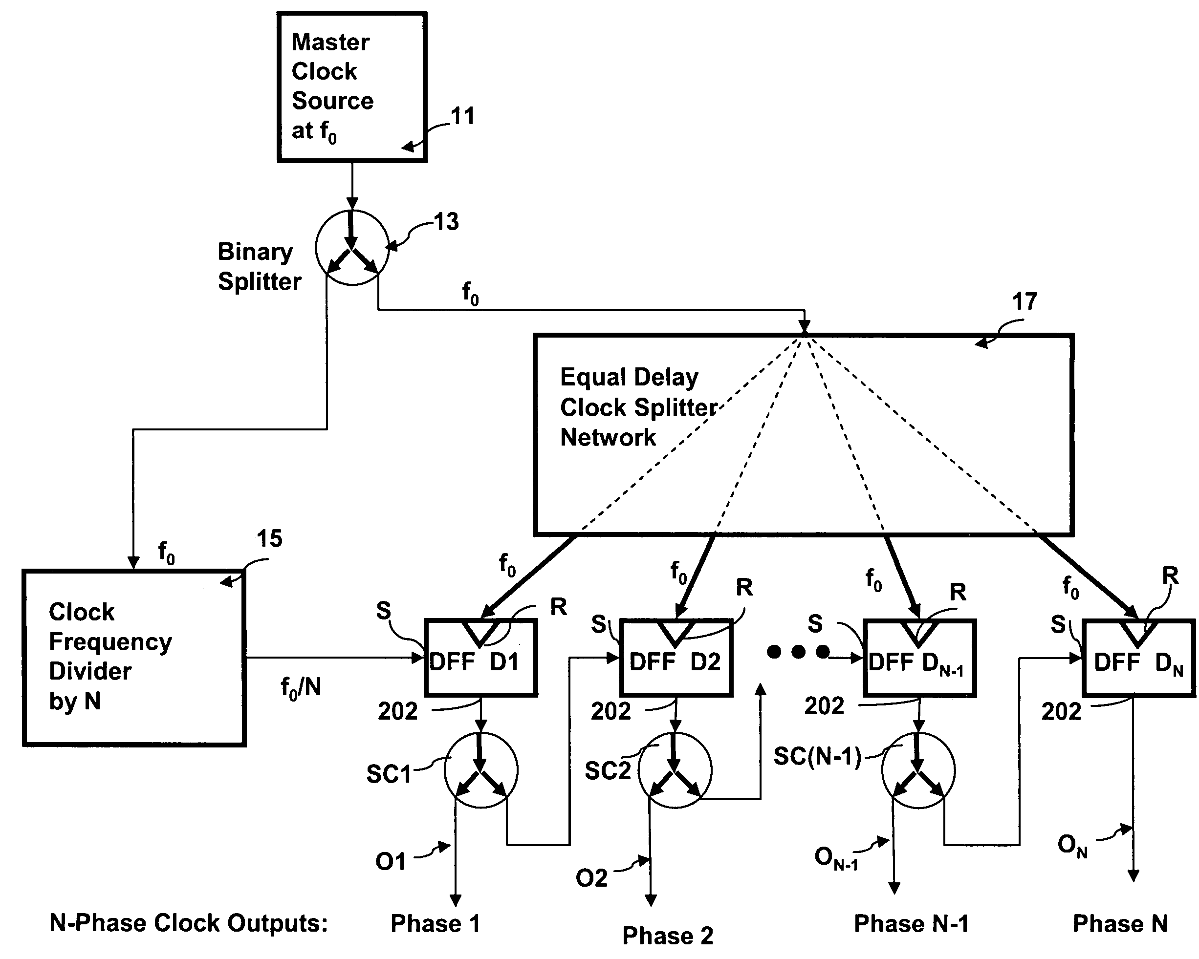
[0029]FIG. 2 is a block diagram of a multiphase clock circuit embodying the invention. A master clock 11 generates a master frequency clock signal fc=fo. The master clock signal is distributed via a binary splitter 13 to a divide by N circuit 15 and a precision clock distribution network 17. The circuit makes use of a chain of clocked data flip-flops (DFFs), together with the master clock frequency divider 15 and the precision clock distribution network 17. The output from the frequency divider, which may be considered a decimated clock pulse, is fed to the data input of the first DFF (DFF D1) of the serial chain of DFFs. The data input is sequentially clocked out from each DFF at the higher master clock rate of fc=fo. Because the DFFs are destructive memory cells that are reset every period, they retain no memory and hence rare errors do not accumulate and / or recirculate.

[0030]The heart of the FIG. 2 circuit includes the series chain of N data flip flops or DFFs which are clocked a...


PUM


Abstract

A multiphase clock circuit in which bit errors are propagated only for the duration of the clock cycle in which a bit error occurs. The circuit recovers automatically from bit errors and is capable of operating at high frequency with high clock precision. The multiphase clock circuit can generate a plurality of clock pulse streams, each pulse stream at the same clock frequency, with fixed phase relationships among the streams. The multiphase clock circuit includes a master clock signal of frequency fc which is applied to a divide by N frequency divider circuit for producing a base clock signal of fc / N. The base clock signal is sequentially applied to the data input of a series chain of N clocked data flip-flops (DFFs) each of which is simultaneously clocked by a clock signal of frequency fc to produce N clock signals of base frequency fc / N separated from each other by a constant time delay T=1 / fc.

Description

BACKGROUND OF THE INVENTION[0001]This invention relates to multi-phase clock circuitry and, in particular, to an improved multiphase clock circuit in which the generation and propagation of clock pulse errors is contained and which clock circuit is highly suitable for use in combination with circuits (e.g., digital IQ mixer circuits) requiring multiphase clocks.[0002]A clock signal in a digital circuit may consist of a periodic time series of pulses, at frequency fclock. In many digital circuits, two or more clock signals are required having the same frequencies but different phases. This can be obtained by shifting the pulses in a given clock signal relative to those in other clock signals by a fixed fraction of a clock period T=1 / fclock. For example, if there are 4 clock signals of like frequency, the clocks are delayed relative to each other by T / 4. That is, clock #2 is delayed from clock #1 by T / 4, clock #3 is delayed from clock #2 by T / 4, and clock #4 is delayed from clock #3 b...

Claims


Application Information

Patent Timeline
Patent Type & Authority Patents(United States)
IPC IPC(8): G06F1/04
CPCG06F1/04G06F1/10H03K5/15093
Inventor KIRICHENKO, DMITRI
Owner HYPRES
Why Eureka
Try Eureka