Output stage circuit and operational amplifier thereof

a technology of output stage and amplifier, which is applied in the field of output stage circuit and an operational amplifier thereof, can solve the problems of circuits that cannot be applied to simple two-stage amplifiers, circuit layouts occupying a lot of layout areas in integrated circuits, and inaccurate resistance and capacitance in integrated circuits. to achieve the effect of reducing the layout area of circuits

Active Publication Date: 2010-08-31
REALTEK SEMICON CORP
View PDF6 Cites 4 Cited by
  • Summary
  • Abstract
  • Description
  • Claims
  • Application Information

AI Technical Summary

Benefits of technology

[0010]The present invention is direct to an output stage circuit for reducing the circuit layout area
[0011]In addition, the present invention is directed to an operational amplifier to reduce the passive element.

Problems solved by technology

1. Two sets of resistor and capacitor (R10, C10) and (R11, C11) should be used in this circuit, and such utilization in an integrated circuit will occupy a lot of layout area, and resistance and capacitance thereof in the integrated circuit are inaccurate.
2. When a higher supply voltage, such as 5V, is applied to this circuit, a folded-cascode configuration FC must be used in the bias circuit B10. Thus, this circuit cannot be applied to simple two stage amplifier.

Method used


Image

  • Output stage circuit and operational amplifier thereof
  • Output stage circuit and operational amplifier thereof
  • Output stage circuit and operational amplifier thereof

Examples


Embodiment Construction

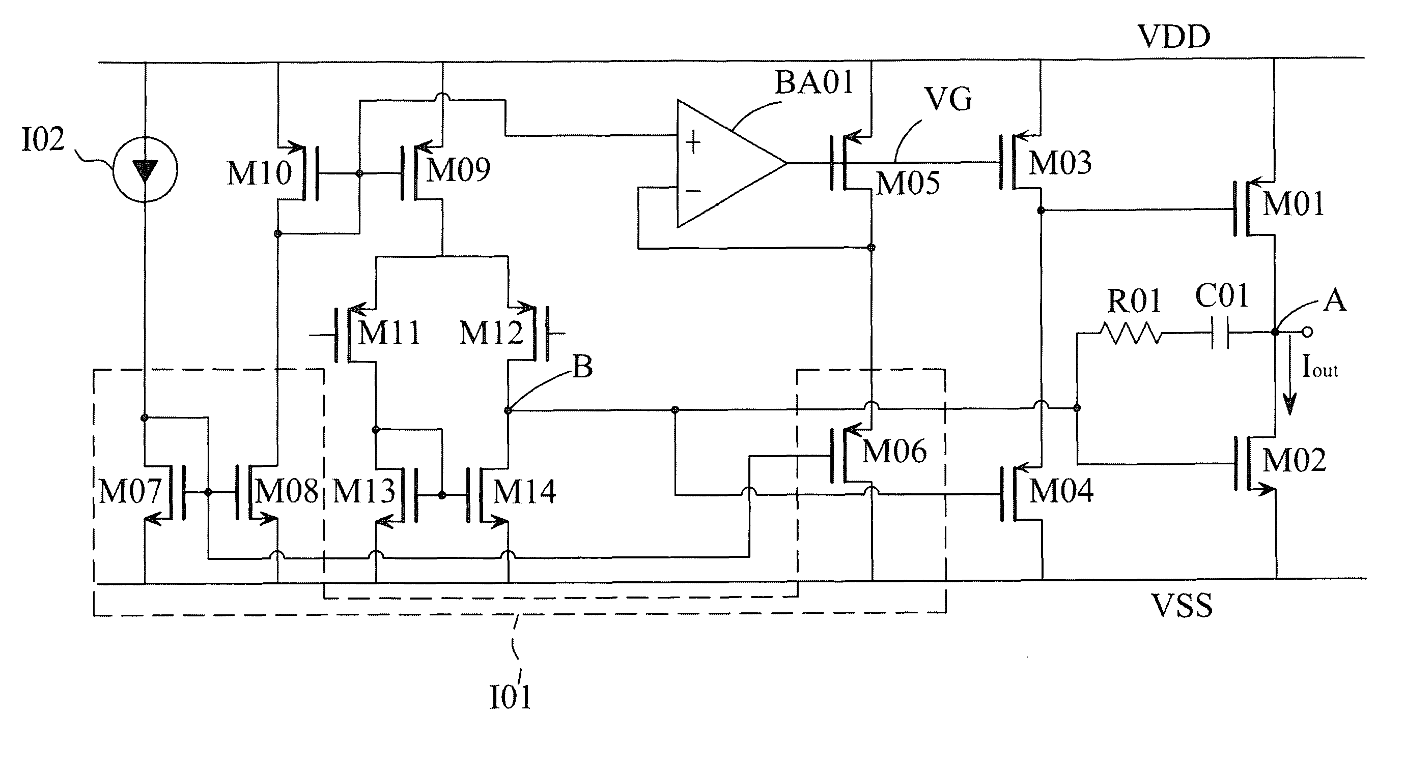
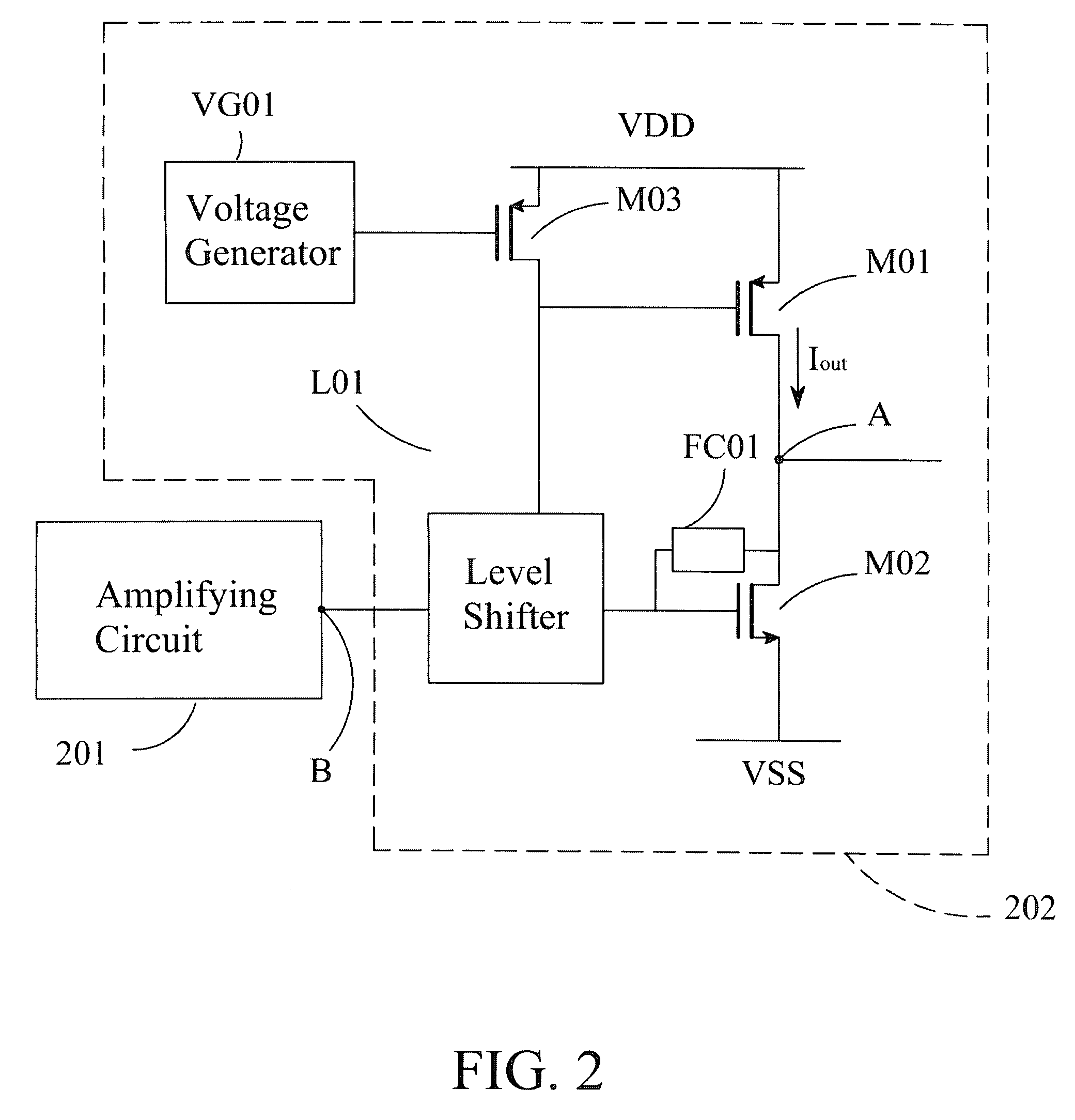
[0020]FIG. 2 illustrates a circuit diagram depicting an operational amplifier according to an embodiment of the present invention. Referring to FIG. 2, the operational amplifier 21 includes an amplifying circuit 201 and an output stage circuit 202, wherein the output stage circuit 202 includes a first transistor M01, a second transistor M02, a third transistor M03, a level shifter L01, a frequency compensating circuit FC01 and a voltage generator VG01. In addition, In order to illustrate the embodiment of the present invention, a node A, a node B, a first common voltage VDD and a second common voltage VSS is further shown in FIG. 2. Generally, the common voltage VDD is a power source voltage, the common voltage VSS is a ground voltage, nevertheless, the present invention is not limited to this embodiment. The first transistor M01 and the second transistor M02 of the output stage circuit 202 is used for driving a load. In the embodiment, for keeping uniformity between the signal outp...


PUM


Abstract

The present invention relates to an output stage circuit and an operational amplifier thereof. In the output stage circuit, one of a gate of a transistor is coupled to a gate of a bias transistor and a level shifter in response to a small signal outputted from an amplifying circuit in the operational amplifier. In addition, a gate voltage of the bias transistor is controlled by a voltage generating circuit to control a DC bias of the transistor of the output stage circuit. Therefore, there is no need extra frequency compensating component for compensating the transistor of the output stage circuit, and to save circuit layout area and cost can be achieved by the present invention.

Description

[0001]This application claims the benefit of the filing date of Taiwan Application Ser. No. “096141792”, filed on “Nov. 6, 2007”, the content of which is incorporated herein by reference.BACKGROUND OF THE INVENTION[0002]1. Field of the Invention[0003]The present invention relates to an amplifier, and more particularly, to an output stage circuit and an operational amplifier thereof.[0004]2. Description of the Related Art[0005]In analog circuit, an output stage circuit plays a role of driving a load in the condition of less gain decreasing.[0006]FIG. 1 illustrates a circuit diagram depicting a complementary metal-oxide semiconductor (CMOS) operational amplifier with class AB output stage 100 in the prior art. Referring to FIG. 1, the operational amplifier 10 includes a class AB output stage 100, two resistors R10 and R11, two capacitors C10 and C11, an amplifying circuit A10 and a bias circuit B10, wherein the bias circuit B10 includes two sub bias circuits B10-1 and B10-2. For the e...

Claims


Application Information

Patent Timeline
Patent Type & Authority Patents(United States)
IPC IPC(8): H03F3/45
CPCH03F1/086H03F3/3022H03F3/45183H03F3/45192H03F2203/30015H03F2203/45526H03F2203/45626H03F2203/45668
Inventor LIU, CHANG-SHUN
Owner REALTEK SEMICON CORP
Why Eureka
Try Eureka