Semiconductor device and manufacturing method thereof

a semiconductor and semiconductor technology, applied in the field of integrated circuits, can solve the problems of judging whether there is a wireless chip or not, and each information of that chip is easily different from each other, so as to prevent forgery of ic tags, improve security, and prevent forgery by rewriting data

Inactive Publication Date: 2010-09-14
SEMICON ENERGY LAB CO LTD
View PDF16 Cites 24 Cited by
  • Summary
  • Abstract
  • Description
  • Claims
  • Application Information

AI Technical Summary

Benefits of technology

[0005]A semiconductor device with a high function and a high added value can be provided by providing a memory circuit (also referred to as a memory, simply) as a circuit integrated over a semiconductor substrate.
[0032]In addition, according to the present invention, forgery of an IC tag can be prevented and security thereof can be improved. A memory circuit in the semiconductor device according to the present invention is written with data by an optical action and an electrical action, is nonvolatile, and is available for adding data. Thus, forgery by rewriting data can be prevented. In addition, new data can be written additionally. That is, the present invention can provide a semiconductor device having a memory element which can not be rewritten.

Problems solved by technology

Therefore, it can only judge whether there is a wireless chip or not.
However, since a wireless chip and a sign or a label are attached separately, each information thereof easily becomes different from each other when a wireless chip is broken or either a wireless chip and an information tag or a label comes unstuck, or is replaced by another.

Method used


Image

  • Semiconductor device and manufacturing method thereof
  • Semiconductor device and manufacturing method thereof
  • Semiconductor device and manufacturing method thereof

Examples


embodiment mode 1

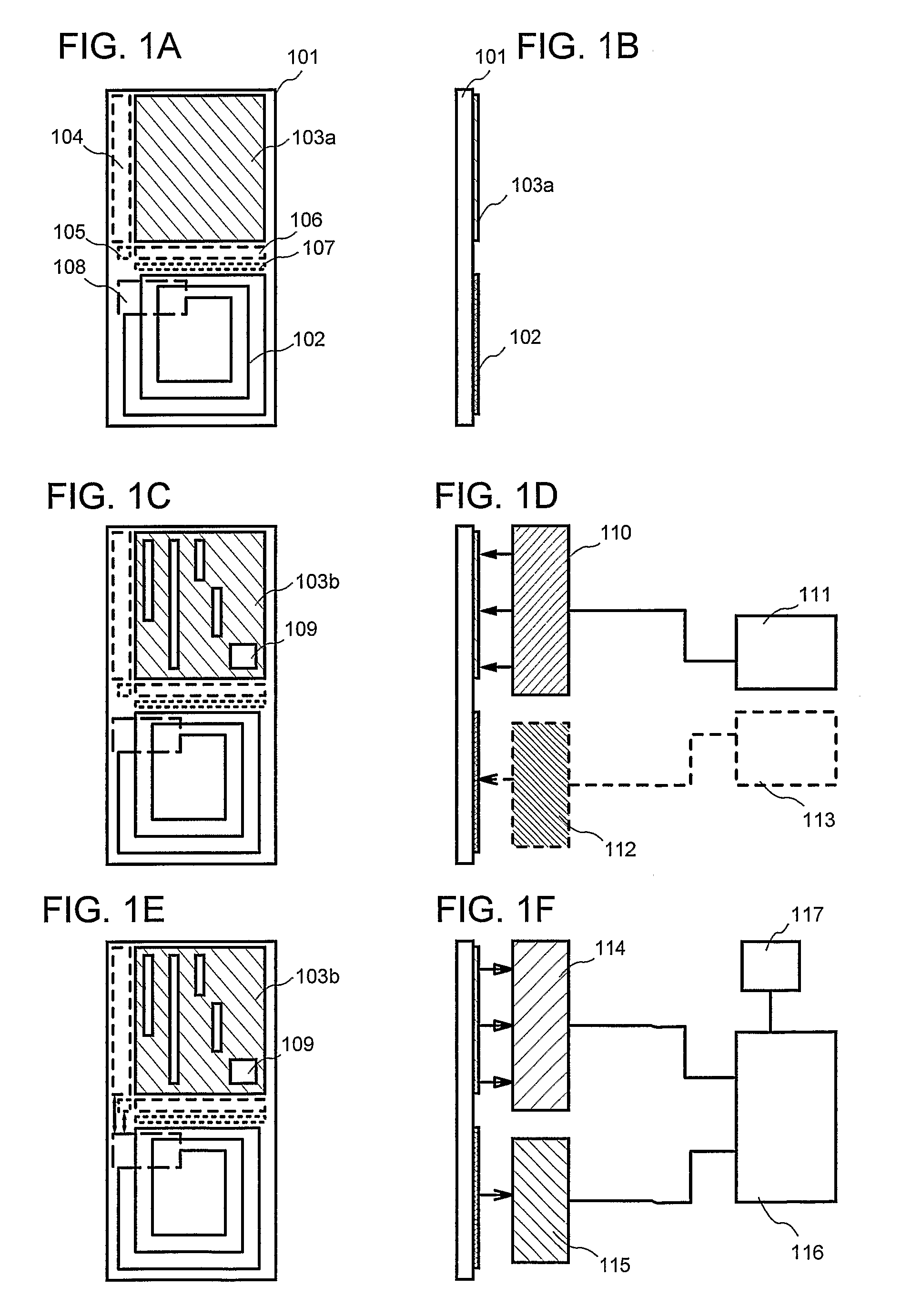
[0049]FIGS. 1A and 1B show an example of a semiconductor device according to the present invention which can send and receive data without contact. FIG. 1A shows a top view of the semiconductor device according to the present invention and FIG. 1B shows a schematic side view of FIG. 1A.

[0050]The semiconductor device according to the present invention shown in FIG. 1A has a structure in which a plurality of circuits (a memory portion and a data sending and receiving portion) is integrated on one base material 101. The memory portion and the data sending and receiving portion are placed to be next to each other so that superposition of noise and interaction between circuits can be reduced. The memory portion has at least a memory cell array 103a having an identification surface, decoder circuits 104 and 105, a selector circuit 106, and a reading and writing circuit 107. The data sending and receiving portion has at least an antenna 102 and an integrated circuit 108 being connected to ...

embodiment mode 2

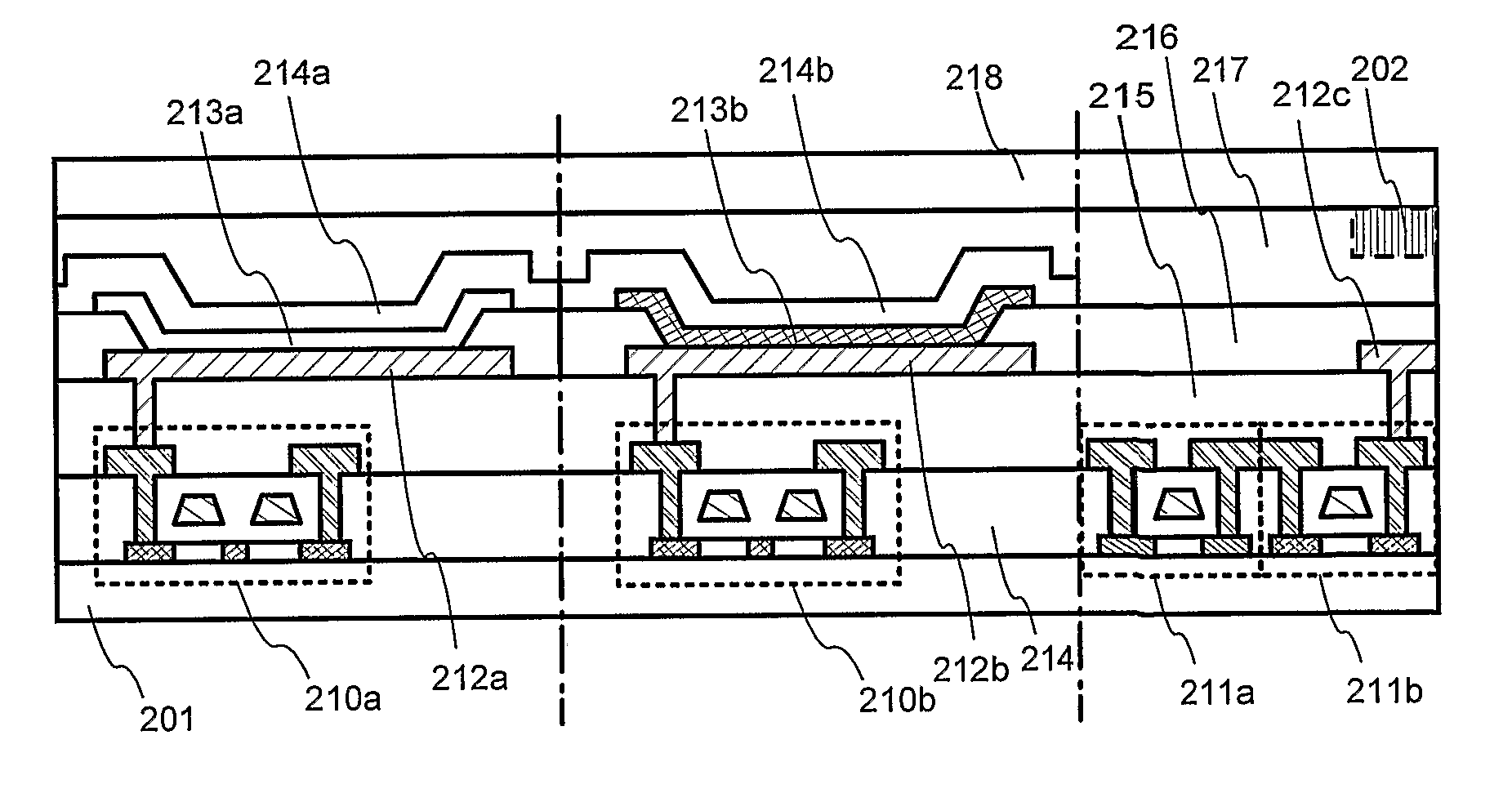
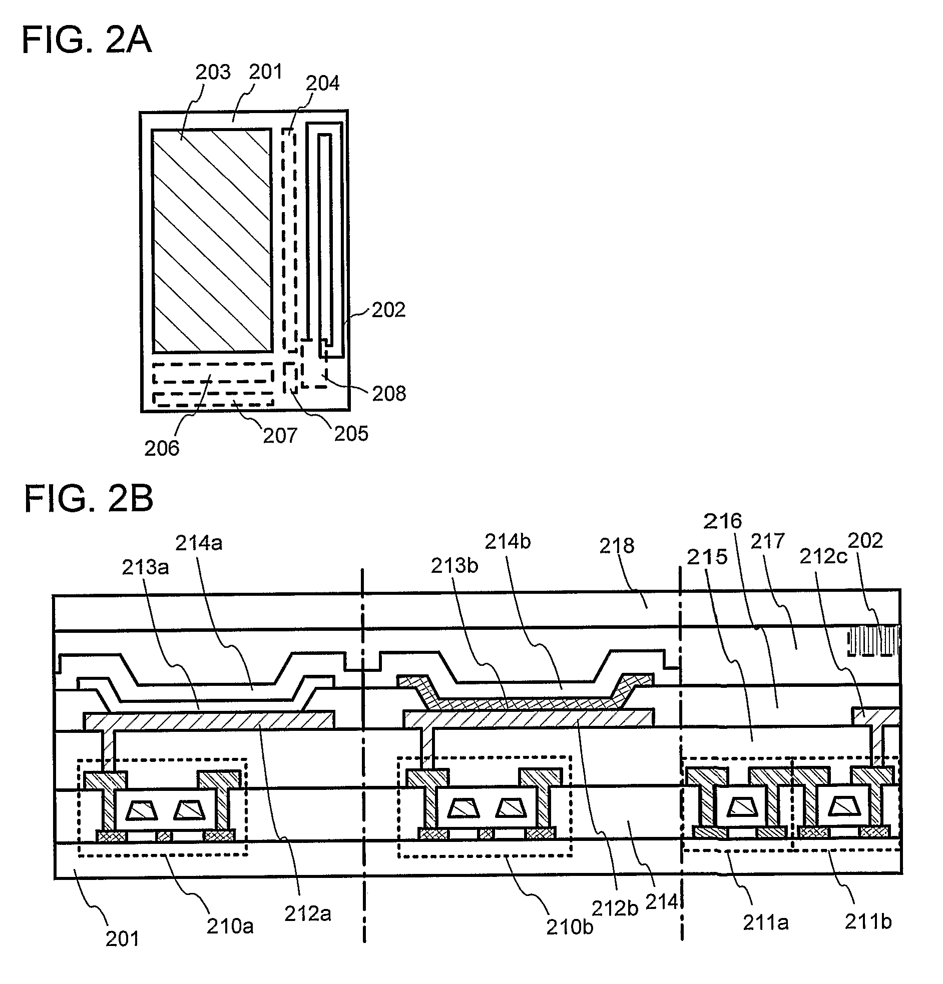
[0071]A semiconductor device according to the present invention has a structure in which a plurality of circuits is integrated and also in which a layer including a plurality of thin film transistors and a layer including a plurality of memory elements are stacked sequentially. In addition, a semiconductor device according to the present invention has a sealing film including a conductive layer which functions as an antenna. The sealing film which serves as an antenna overlaps the edge of the layer including a plurality of memory elements.

[0072]FIG. 2A shows an example of a top view of a semiconductor device according to the present invention. The memory portion has at least a memory cell array 203 having an identification surface, decoder circuits 204 and 205, a selector circuit 206, and a reading and writing circuit 207. The data sending and receiving portion has at least an integrated circuit 208 being connected to an antenna. The circuits are provided on the common base material...

embodiment mode 3

[0090]FIG. 4 is a block diagram of the semiconductor device according to the present invention.

[0091]As shown in FIG. 4, a semiconductor device 20 surrounded by a dotted line can exchange data without contact. The semiconductor device 20 has a power source circuit 11, a clock generator circuit 12, a data demodulator / modulator circuit 13, a controlling circuit 14 for controlling other circuits, an interface circuit 15, a memory circuit 16, a data bus 17, and an antenna (antenna coil) 18.

[0092]The power source circuit 11 is a circuit for generating electric current and electric voltage which is supplied to each circuit inside the semiconductor device 20 based on an alternating signal from the antenna 18. The clock generator circuit 12 is a circuit for generating various clock signals which are supplied to each circuit in the semiconductor device 20 based on an alternating signal inputted from the antenna 18. The data demodulator / modulator circuit 13 has a function for demodulating / mod...


PUM


Abstract

It is an object of the present invention to provide a semiconductor device having a memory circuit which is nonvolatile and able to be written additionally, an antenna which can be easily manufactured, and to provide a manufacturing method thereof. In addition, it is an object of the present invention to prevent unauthorized rewriting of information of a wireless chip and forgery of a wireless chip itself and to ensure a security of a wireless chip. In view of the foregoing, the present invention provides an IC tag in which information thereof is identified by wireless communication signal and also information of a memory in an IC tag (a memory which can not be rewritten) is identified by an optical reading device. A memory in an IC tag according to the present invention has an identification surface with which information can be identified by an optical reading device.

Description

TECHNICAL FIELD[0001]The present invention relates to an integrated circuit having an antenna and a memory for identifying and management of goods, merchandise, and people. More specifically, the present invention relates to a wireless IC tag such as a wireless IC tag and related goods.BACKGROUND ART[0002]A barcode can be nominated as an object for identifying goods. The barcode is printed on goods directly by flexography (a printing method using a relief plate made of rubber or flexible synthetic resin), offset printing, gravure printing, and the like; or printed on a label first, before being attached to goods. By using a barcode, data of a barcode (price or name of merchandise) can be read by an optical reading device also called a barcode reader. According to the data, management of the sales volume, stocks, and distribution can be conducted. However, there are problems of a barcode in terms of information and function, for example, a number of digits is small and security is no...

Claims


Application Information

Patent Timeline
Patent Type & Authority Patents(United States)
IPC IPC(8): G06K19/06
CPCB82Y10/00G11C13/0007G11C13/0014G11C17/16H01L27/10H01L27/28H01L27/283G11C13/0004G11C2213/32G11C2213/77G11C2213/79H01L27/12H01L29/78645H01L51/0059H10K19/10H10K85/631H10K19/80H10K19/00
Inventor ABE, HIROKOYUKAWA, MIKIONOMURA, RYOJISEO, SATOSHIYAMAZAKI, SHUNPEI
Owner SEMICON ENERGY LAB CO LTD
Why Eureka
Try Eureka