Printed circuit board having structure for relieving stress concentration, and semiconductor chip package equipped with the same

a printed circuit board and stress concentration technology, which is applied in the direction of printed circuit stress/warp reduction, sustainable manufacturing/processing, final product manufacturing, etc., to achieve the effect of relieving stress concentration

Inactive Publication Date: 2010-09-28
HAESUNG CO LTD
View PDF18 Cites 1 Cited by
  • Summary
  • Abstract
  • Description
  • Claims
  • Application Information

AI Technical Summary

Benefits of technology

[0014]The present invention provides a printed circuit board having a structure for relieving a stress concentration on corner leads that are arranged on the printed circuit board, due to a difference in thermal expansion coefficients between a semiconductor device and the printed circuit board when the semiconductor device is mounted on the printed circuit board. Also, the present invention provides a semiconductor chip package equipped with the same printed circuit board.

Problems solved by technology

Such concentration of the peel stress results in breakage of the leads.

Method used


Image

  • Printed circuit board having structure for relieving stress concentration, and semiconductor chip package equipped with the same
  • Printed circuit board having structure for relieving stress concentration, and semiconductor chip package equipped with the same
  • Printed circuit board having structure for relieving stress concentration, and semiconductor chip package equipped with the same

Examples


Embodiment Construction

[0028]Hereinafter, embodiments of the present invention will be described in detail with reference to the appended drawings.

[0029]FIG. 4 is a view for explaining a stress relief structure of a printed circuit board according to the present invention.

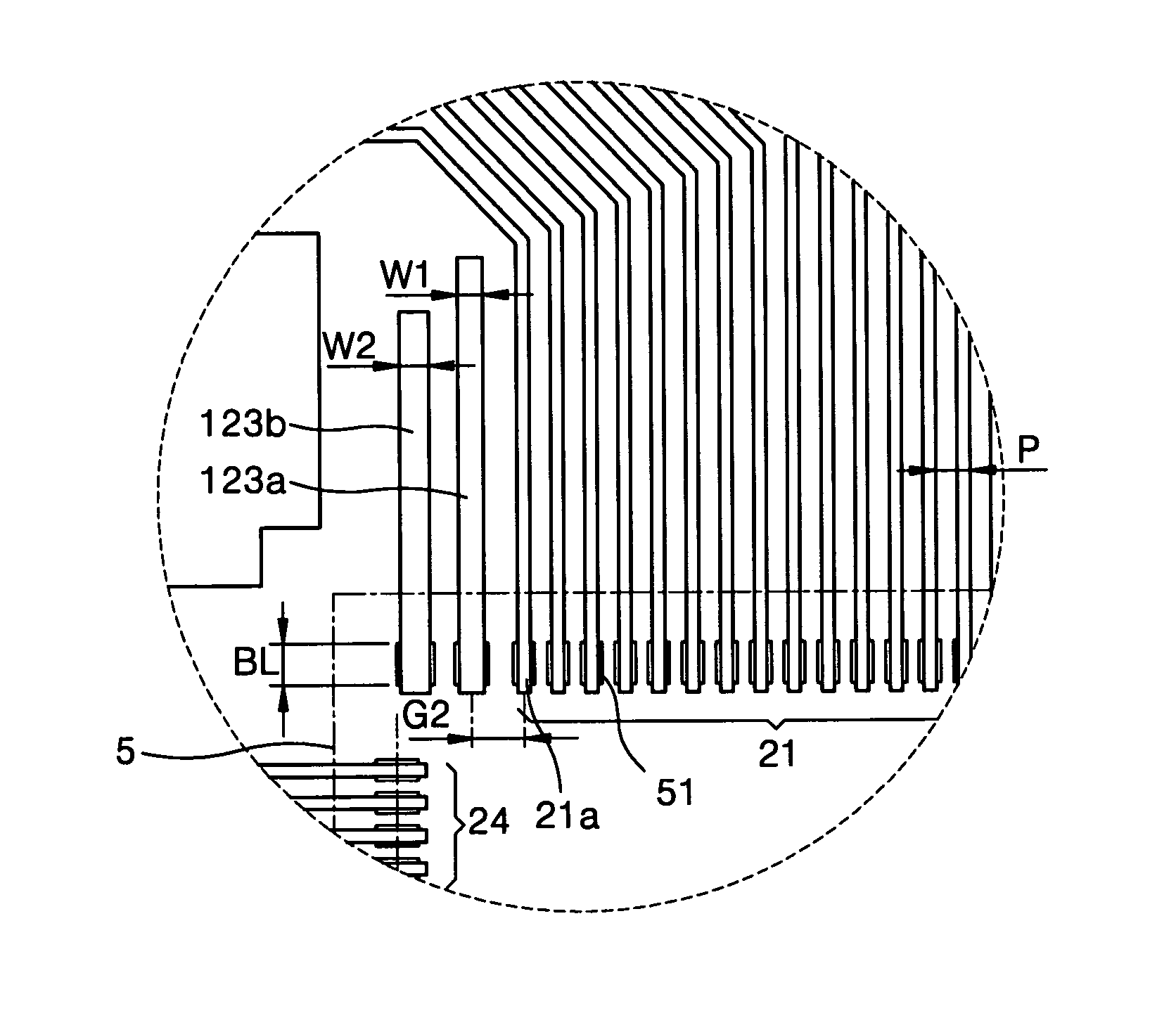
[0030]Referring to FIG. 4, when a semiconductor device 5 is mounted on the printed circuit board, in order to relieve the stress concentration on the leads located near the corners of the semiconductor device 5, an additional lead 123a is formed adjacent to the outer most lead of leads 21. The additional lead 123a has a width wider than that of each of the leads 21.

[0031]If the leads 21 are formed in parallel with a same pitch P smaller than 30 μm on the printed circuit board, the additional lead 123a will have a wider width of 20 μm or more according to the size of the semiconductor device 5.

[0032]It is preferable that an edge gap G2 between the additional lead 123a and an outer most lead 21a of the leads 21 is smaller than 0.8 mm in or...


PUM


Abstract

There are provided a printed circuit board having a structure for relieving a stress concentration on an outer most lead of leads, due to a difference in thermal expansion coefficients between the semiconductor device and the printed circuit board when the semiconductor device is mounted on the printed circuit board. The printed circuit board includes an inner lead portion to be connected to the semiconductor device. The inner lead portion includes a plurality of leads, arranged in parallel with a same pitch in a predetermined area, and additional leads located near both ends of the predetermined area in which the plurality of leads are arranged in parallel, respectively, wherein each of the plurality of leads has a pitch smaller than 30 μm and a width of the additional lead is wider than 20 μm. There are also provided a semiconductor chip package equipped with the printed circuit board according to the present invention.

Description

[0001]This application claims the priority of Korean Patent Application No. 10-2004-0057141, filed on Jul. 22, 2004, in the Korean Intellectual Property Office, the disclosure of which is incorporated herein in its entirety by reference.BACKGROUND OF THE INVENTION[0002]1. Field of the Invention[0003]The present invention relates generally to a printed circuit board and a semiconductor chip package with the same, and more particularly, to a printed circuit board having a structure for relieving a stress concentration on corner leads that are connected to a semiconductor device on the printed circuit board, and a semiconductor chip package equipped with the same printed circuit board.[0004]2. Description of the Related Art[0005]FIG. 1 is a top view of a flexible printed circuit board 1 connected to a display module of a liquid crystal display device, as an example of a printed circuit board on which a semiconductor device is mounted.[0006]Referring to FIG. 1, an external connection te...

Claims


Application Information

Patent Timeline
Patent Type & Authority Patents(United States)
IPC IPC(8): H01R9/00
CPCH01L23/49838H05K1/111H05K1/0271H05K1/189H05K2201/09781H01L2924/0002H05K2201/10674H01L2924/00Y02P70/50H05K1/02
Inventor JANG, CHANG-SOORYU, JAE-CHULHAN, SEONG-YOUNG
Owner HAESUNG CO LTD
Why Eureka
Try Eureka