
Process for producing silicon carbide crystals having increased minority carrier lifetimes

a silicon carbide crystal and lifetime technology, applied in the direction of crystal growth process, after-treatment details, condensed vapor, etc., can solve the problems of affecting the blocking voltage of the device, the utilization of the device beyond certain parameters, and the low specific on-resistance of the sic-based device, so as to reduce the concentration of minority carrier recombination centers, increase minority carrier lifetimes, and control the effect of intrinsic defects

Active Publication Date: 2010-10-12
CREE INC
View PDF17 Cites 0 Cited by
  • Summary
  • Abstract
  • Description
  • Claims
  • Application Information

AI Technical Summary

Benefits of technology

The present invention is about a process for producing silicon carbide crystals with increased minority carrier lifetimes. By controllably decreasing the number of defects and resulting deep level states in the crystal, the process reduces the concentration of minority carrier recombination centers, which act as recombination centers for minority carriers. This results in a material with increased minority carrier lifetimes. The process involves heating the crystal to a high temperature and then cooling it at a slow rate to remove the defects. The resultant silicon carbide crystals have increased minority carrier lifetimes, which make them useful in the production of semiconductor devices such as power devices.

Problems solved by technology

Although silicon (Si) has been the material of choice for many semiconductor applications, its fundamental electronic structure and characteristics prevent its utilization beyond certain parameters.
This allows much higher doping and a much thinner drift layer for a given blocking voltage, resulting in a very low specific on-resistance in SiC-based devices.
Although it has a much higher breakdown field than silicon, SiC has lower hole and electron mobilities and shorter minority carrier lifetimes, which can detrimentally affect the blocking voltage for a device as voltages increase.
The production of suitably thick epitaxially grown SiC crystals, however, is not currently cost effective.
Moreover, it can be undesirably time consuming to manufacture such crystals.
As noted above, however, bulk SiC single crystals can have relatively short minority carrier lifetimes. As such, these materials typically are less suitable for use in certain applications, including power devices.

Method used


Image

  • Process for producing silicon carbide crystals having increased minority carrier lifetimes
  • Process for producing silicon carbide crystals having increased minority carrier lifetimes
  • Process for producing silicon carbide crystals having increased minority carrier lifetimes

Examples


Embodiment Construction

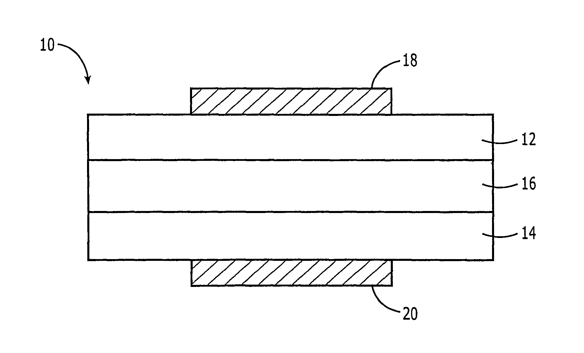
[0024]The present invention now will be described more fully hereinafter with reference to the accompanying drawings, in which some, but not all embodiments of the invention are shown. Indeed, this invention may be embodied in many different forms and should not be construed as limited to the embodiments set forth herein; rather, these embodiments are provided so that this disclosure will satisfy applicable legal requirements. Like numbers refer to like elements throughout.

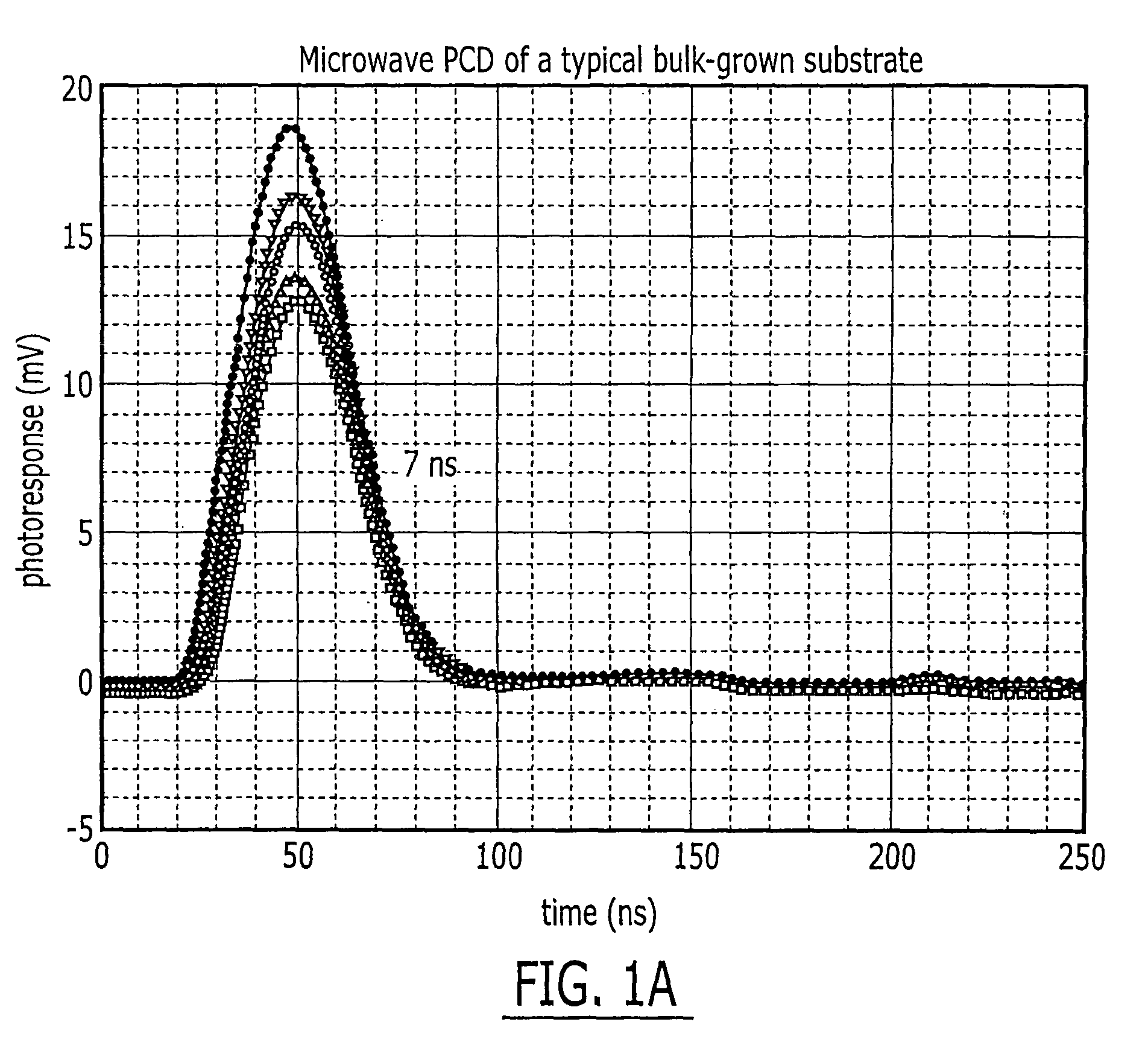
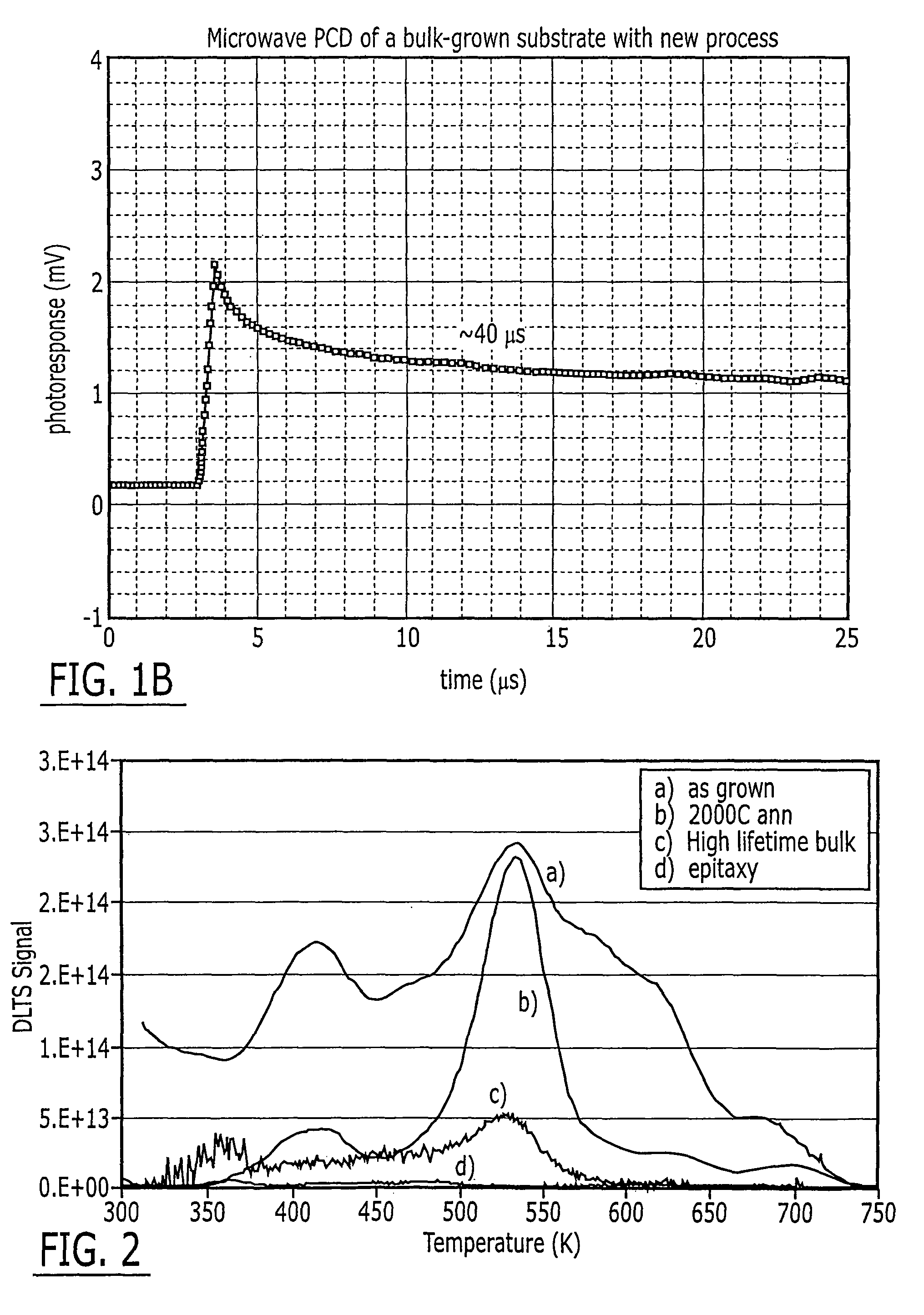
[0025]As used herein and as understood in the art, the term “minority carrier recombination centers” refers to recombination centers that form in a silicon carbide crystal during the growth process owing to the presence of intrinsic defects or associations thereof. Intrinsic defects can occur in bulk grown and epitaxially grown silicon carbide materials. Intrinsic defects are also referred to in the art as “point defects” and include all defects that contain at least one intrinsic component, for example, interstit...


PUM

PropertyMeasurementUnit
temperatureaaaaaaaaaa

Abstract

A process is described for producing silicon carbide crystals having increased minority carrier lifetimes. The process includes the steps of heating and slowly cooling a silicon carbide crystal having a first concentration of minority carrier recombination centers such that the resultant concentration of minority carrier recombination centers is lower than the first concentration.

Description

CROSS-REFERENCE TO RELATED APPLICATIONS[0001]This application claims priority from provisional application Ser. No. 60 / 639,154 filed Dec. 22, 2004, which is hereby incorporated entirely herein by reference.STATEMENT OF GOVERNMENT INTEREST[0002]This invention was developed under ONR Contract No. N00014-02-C-0302. The government may have certain rights in this invention.BACKGROUND OF THE INVENTION[0003]The present invention relates to a process for the production of silicon carbide crystals and more particularly to the production of silicon carbide crystals having increased minority carrier lifetimes.[0004]Semiconductor devices are increasingly required to accommodate high currents and / or high voltages without failing. Many high power applications call for the use of a semiconductor switch which is required to conduct a large current when turned on, and to block a high voltage when off. Although silicon (Si) has been the material of choice for many semiconductor applications, its fund...

Claims


Application Information

Patent Timeline
Patent Type & Authority Patents(United States)
IPC IPC(8): H01L21/31
CPCC30B29/36C30B33/02C30B11/003
Inventor CARTER, JR., CALVIN H.JENNY, JASON R.MALTA, DAVID P.HOBGOOD, HUDSON M.TSVETKOV, VALERI F.DAS, MRINAL K.
Owner CREE INC
Features
  • Generate Ideas
  • Intellectual Property
  • Life Sciences
  • Materials
  • Tech Scout
  • Unparalleled Data Quality
  • Higher Quality Content
  • 60% Fewer Hallucinations
Learn More