
Thermal treatment of silicon wafers useful for photovoltaic applications

a technology of photovoltaic applications and silicon wafers, applied in the field of thermal treatment of silicon wafers, can solve the problems of reducing the solubility limit of equilibrium oxygen, super-saturating oxygen incorporated at the interface during growth, and lowering the lifetime of minority carrier silicon, so as to achieve the effect of increasing the lifetime of minority carrier

Active Publication Date: 2015-08-11
GTAT IP HLDG
View PDF3 Cites 0 Cited by
  • Summary
  • Abstract
  • Description
  • Claims
  • Application Information

AI Technical Summary

Benefits of technology

The patent describes a process for improving the quality of silicon wafers used in solar cells. By briefly annealing the wafer in a high-temperature, oxygen-containing environment, the process dissolves any impurities in the crystal structure. This increases the lifespan of minority carriers, which are important for the performance of photovoltaic solar cells. The cooling process is done quickly, without any holding period, to ensure optimal results.

Problems solved by technology

However, as the ingot gradually cools as it is slowly drawn from the melt, the equilibrium oxygen solubility limit decreases and oxygen incorporated at the interface during growth becomes super saturated.
However, these oxygen precipitates (also referred to as gettering sites) throughout the entire wafer dramatically lower the minority carrier recombination lifetime of silicon, which is critically important for solar cells.
However, FZ silicon is prohibitively expensive and is not used in commercial-scale terrestrial solar cell applications.
For CZ silicon, various techniques are applied to reduce the oxygen concentration in the ingot to below 13 ppma but the techniques introduce operational constraints and have not been completely successful.
For all IC types, low oxygen precipitation in the active surface region is not desired.
Further, because almost all the IC's made today are majority carrier devices, such as MOSFET's, minority carrier lifetime is not considered to be very important.
The Falster process is believed to prevent oxygen precipitation near the surface regions and thus does not enjoy the advantages of interior oxygen precipitation described above for the denuded zone process.

Method used


Image

  • Thermal treatment of silicon wafers useful for photovoltaic applications
  • Thermal treatment of silicon wafers useful for photovoltaic applications

Examples


Embodiment Construction

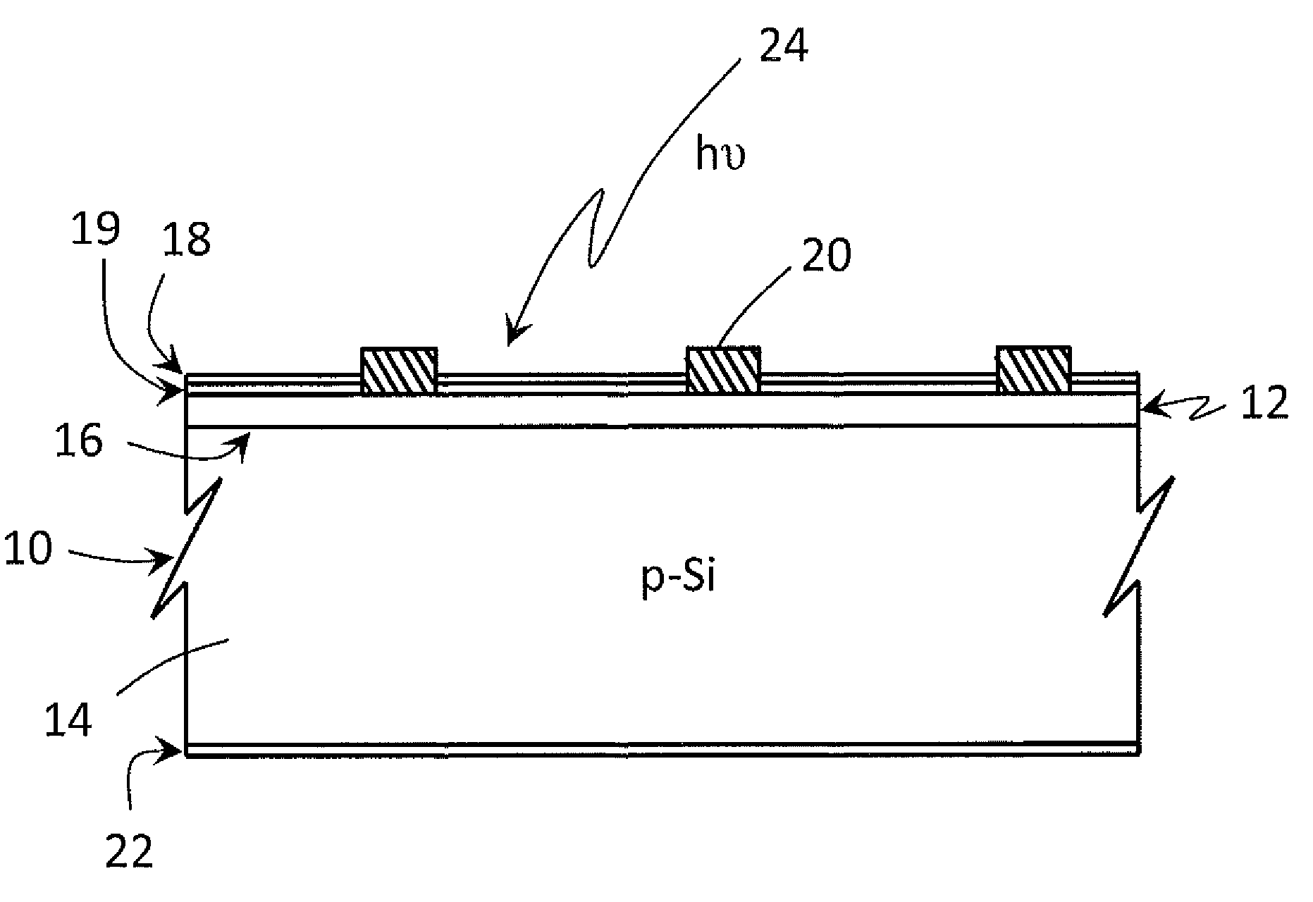
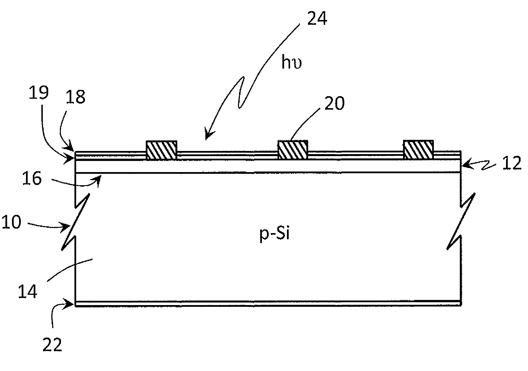
[0018]The need for highly efficient solar cells imposes somewhat different requirements on silicon wafers used for PV applications than for wafers used for integrated circuits. One of the prime requirements for wafers for PV applications is a high minority carrier lifetime (mcl) since the product of the square root of the met multiplied by the diffusion coefficient of the minority carrier determines the distance over which the photo-generated minority carriers in PV cells can effectively diffuse before recombining with majority carriers. The greater this diffusion distance, the higher the probability that the minority carrier will reach the p-n junction (referred to as the solar cell emitter) without recombining with the abundant majority carriers in the silicon. Long lifetime is necessary but not sufficient. Several other requirements need be satisfied for single crystal silicon wafers to be useful in PV applications, such as proper resistivity, low carbon concentration, large diam...


PUM

PropertyMeasurementUnit
temperatureaaaaaaaaaa
temperaturesaaaaaaaaaa
partial pressureaaaaaaaaaa

Abstract

Efficiency of silicon photovoltaic solar cells is increased by an annealing process for immobilizing oxygen formed in Czochralski-grown silicon. The annealing process includes a short anneal in a rapid thermal annealing chamber at a high temperature, for example, greater than 1150° C. in an oxygen-containing ambient. More preferably, the wafer is rapidly cooled to less than 950° C. without an intermediate temperature hold, at which temperature oxygen does not nucleate and / or precipitate. Subsequent processing to form a photovoltaic structure is typically performed at relatively low temperatures of less than 1000° C. or even 875° C.

Description

CROSS-REFERENCE TO RELATED APPLICATIONS[0001]The present application claims the benefit of U.S. Provisional Patent Application No. 61 / 476,371, filed Apr. 18, 2011.BACKGROUND OF THE INVENTION[0002]1. Field of the Invention.[0003]The invention relates generally to thermal treatment of silicon wafers. In particular, the invention relates to thermal treatment of silicon wafers to be used to make photovoltaic cells.[0004]2. Description of the Related Art.[0005]There is currently great interest and intense development in photovoltaic (PV) solar cells which directly convert solar radiation to electrical power. Although many different configurations and even different semiconductor materials have been proposed, an efficient and economical solar cell can be fabricated using structures, materials, and techniques long known for silicon integrated circuits. Specifically, a single crystal or multi-crystalline silicon wafer is processed to have a large-area p-n junction extending across a substan...

Claims


Application Information

Patent Timeline
Patent Type & Authority Patents(United States)
IPC IPC(8): H01L31/0264H01L31/18H01L31/068
CPCH01L31/068H01L31/1864Y02E10/547Y02P70/50
Inventor DELUCA, JOHN P.
Owner GTAT IP HLDG
Features
  • Generate Ideas
  • Intellectual Property
  • Life Sciences
  • Materials
  • Tech Scout
  • Unparalleled Data Quality
  • Higher Quality Content
  • 60% Fewer Hallucinations
Learn More